
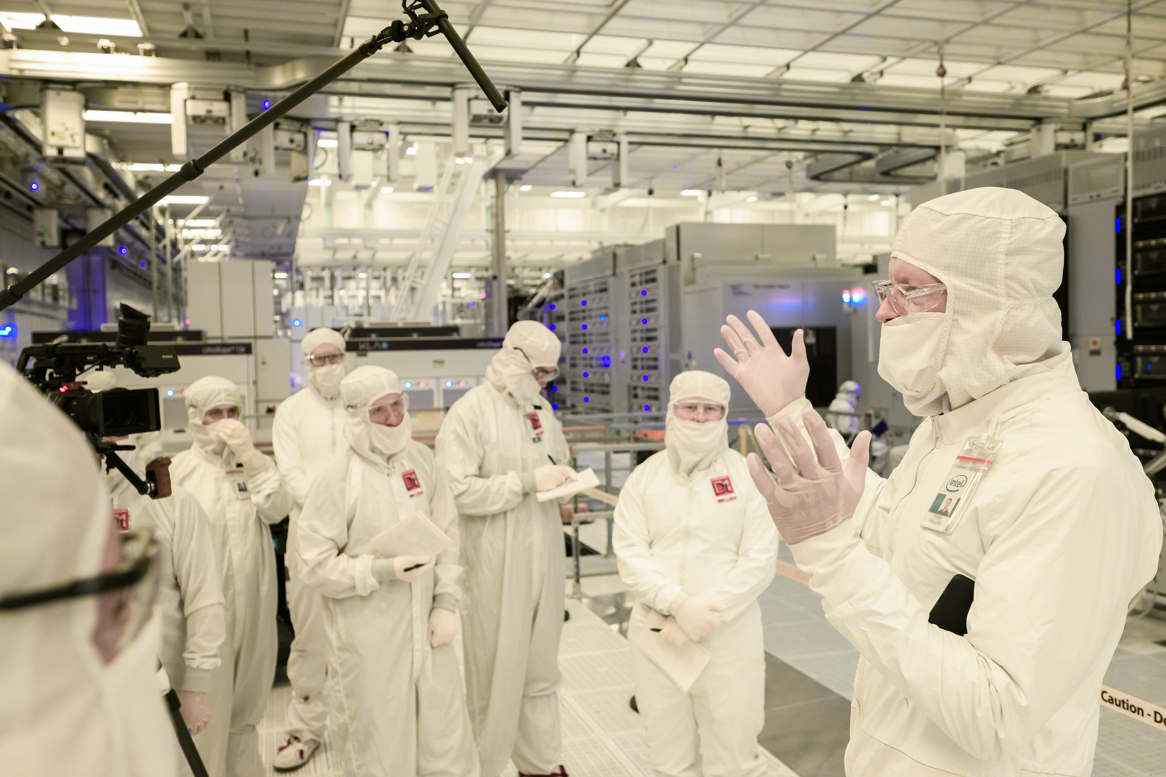
In April 2024 I pulled on a bunny suit at Intel’s D1X fab in Hillsboro, Oregon, and stood a few feet from a machine the size of a bus and worth a small nation state. Intel Fellow Mark Phillips explained this was ASML’s first High-NA EUV scanner, 165 tons of it. Installation had just wrapped and calibration had begun, but realistically still another few months before test wafers could be run. Intel were actually only a few weeks ahead of ASML in terms of installing a tool, enabling a close collaboration between the two.
As we toured the tool, about 15 of us or so with CNBC wielding a pre-approved camera setup, the question was if/when this tool was ever going to be involved in production silicon and hardware.
The answer landed on July 15, 2026. ASML put out a press release confirming that Intel Foundry has taken High-NA into high-volume manufacturing. Using the tool, Intel is patterning a subset of layers on some of its newest notebook processors: these are Panther Lake, the Core Ultra Series 3 laptop parts built on Intel 18A.
From Intel and ASML’s point of view, it means those High-NA layers are dual-qualified in Oregon, and yielding on par with the regular EUV tools that require multiple steps to do the same thing. I asked if this was just test chips, but Intel confirmed it means that notebooks with silicon partly printed on a $380 million High-NA scanner are heading to customers now.
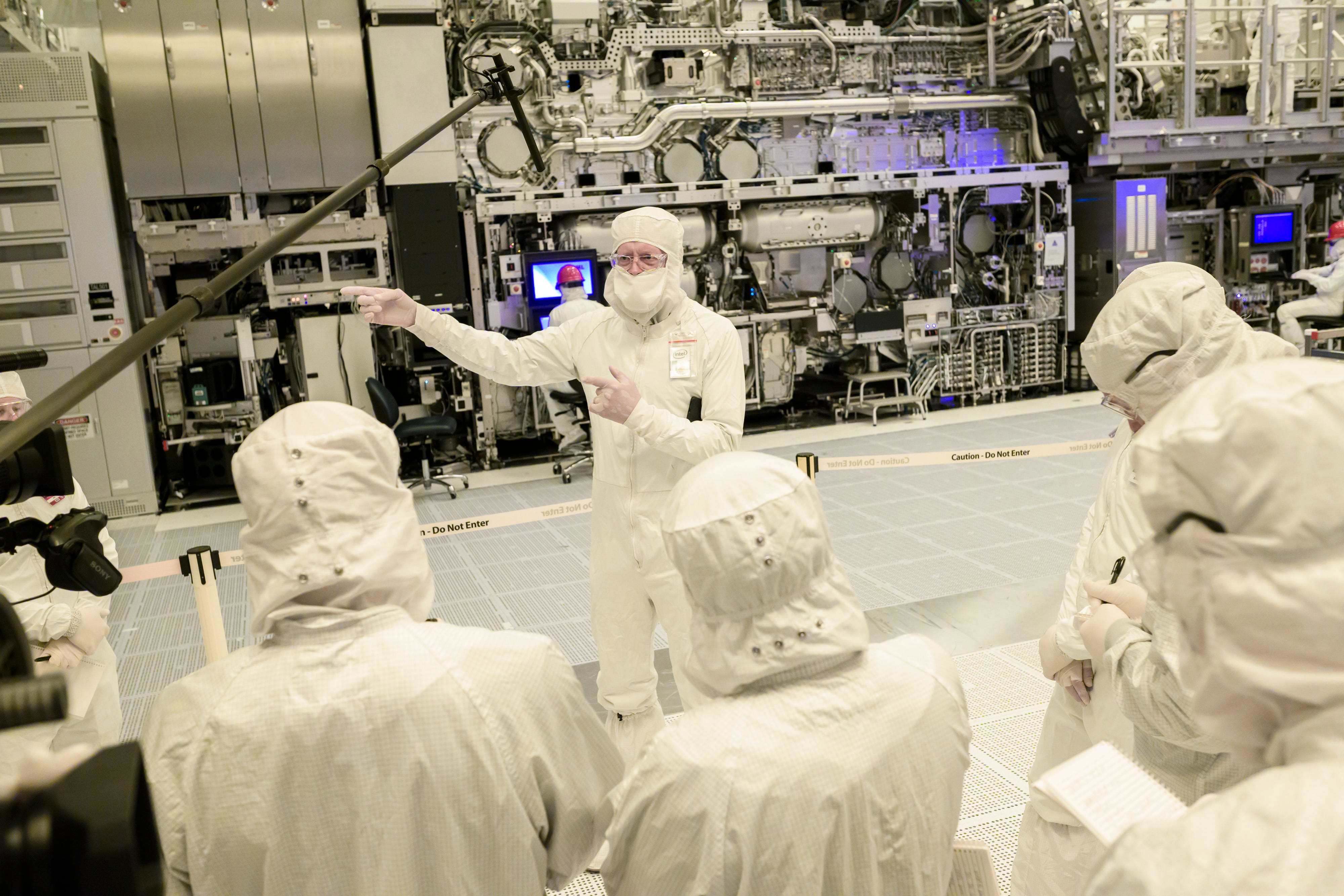
Intel has been able to say it owns the world’s first High-NA tool since that 2024 tour, but there has always been a question of using tools like this for research time over production time. Getting product layers through the machine at a yield that matches the mature scanner one bay over is a big step to overcome, the next question is if the economics of a single pass on a more expensive machine work out long term.
What the machine actually is
The machine is a two-storey wall of stainless pipework, vacuum vessels and cabling wrapped around a wafer stage, and almost all of it is to serve one number in physics. Every EUV scanner in production until now has imaged through optics with a Numerical Aperture (NA) of 0.33. Numerical aperture describes how wide a cone of light the optics can gather, and a wider cone resolves finer detail, so raising it to 0.55 with High-NA sharpens the smallest single-exposure feature by roughly a third. In practice that lets a fab print in a single cycle a pattern that would need two or three aligned Low-NA exposures stitched together. Each exposure removed takes its cost, its cycle time, and one of its defect opportunities with it – in short, fewer exposures are usually better.
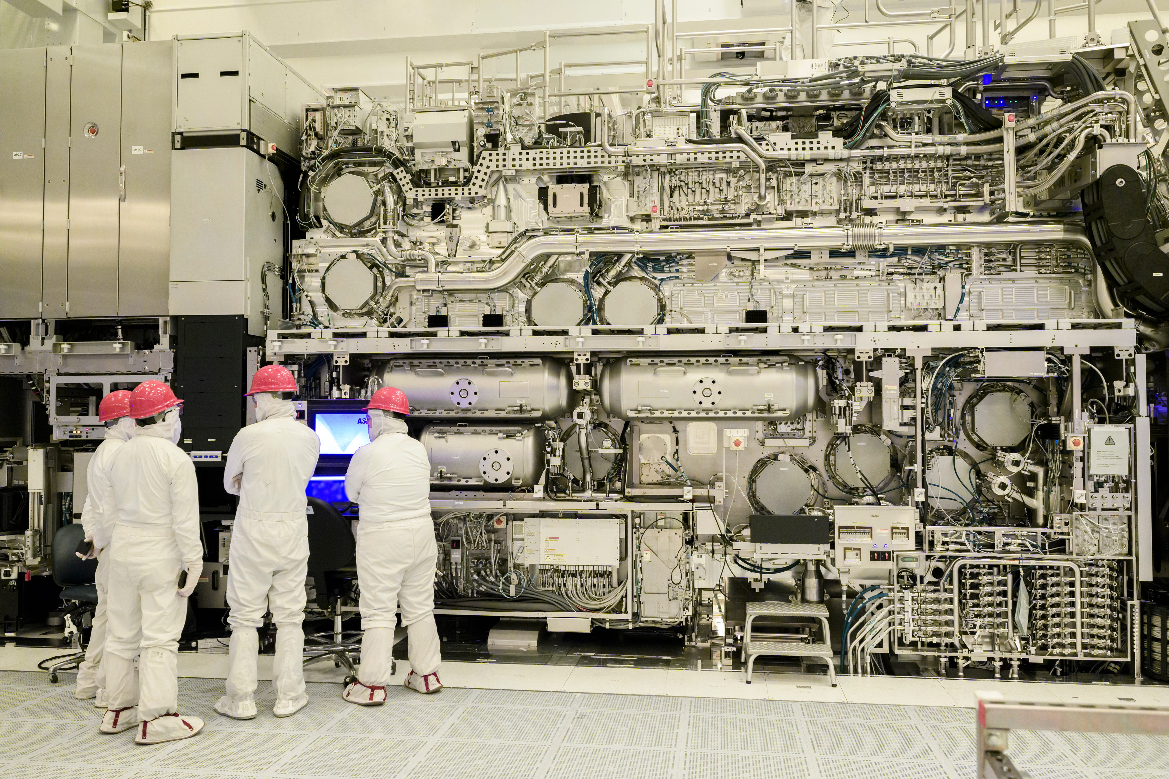
Reaching 0.55 was not free, not only with the machine cost but with physics and chip production as well. ASML moved to camera-style anamorphic optics that magnify the mask by different amounts along the two axes – in literal terms this halves the field that the scanner can image in a single shot. Instead of an 858 mm2 chip, or 26 x 33 millimetres, the maximum an EUV machine can do is 429 mm2, or 26 by 16.5 millimeters.
A full-reticle die now has to be exposed in two halves and stitched back together, which complicates some of the process simplicity the higher resolution was meant to provide.
A single system costs close to $380 million, roughly 2-3 times a Low-NA scanner, and installing one runs to around 250 crates and several months of work on site. Those two facts, a high per-tool cost and a per-exposure penalty set against fewer process steps, have called into question its pricing efficacy.
Where High-NA belongs on the roadmap
Where High-NA will do its real work is longer term – as shown by imec’s long term roadmap. On that timeline, 0.33 NA EUV carries the metal-pitch scaling from the N7 era down to about N2, taking pitch from roughly 40 nm to around 21. Compare that to High-NA 0.55 EUV, we extend down to A14 and through to A5 or so. In roadmap terms High-NA is a decade-long tool whose job begins in earnest soon but will carry through into the 2030s.
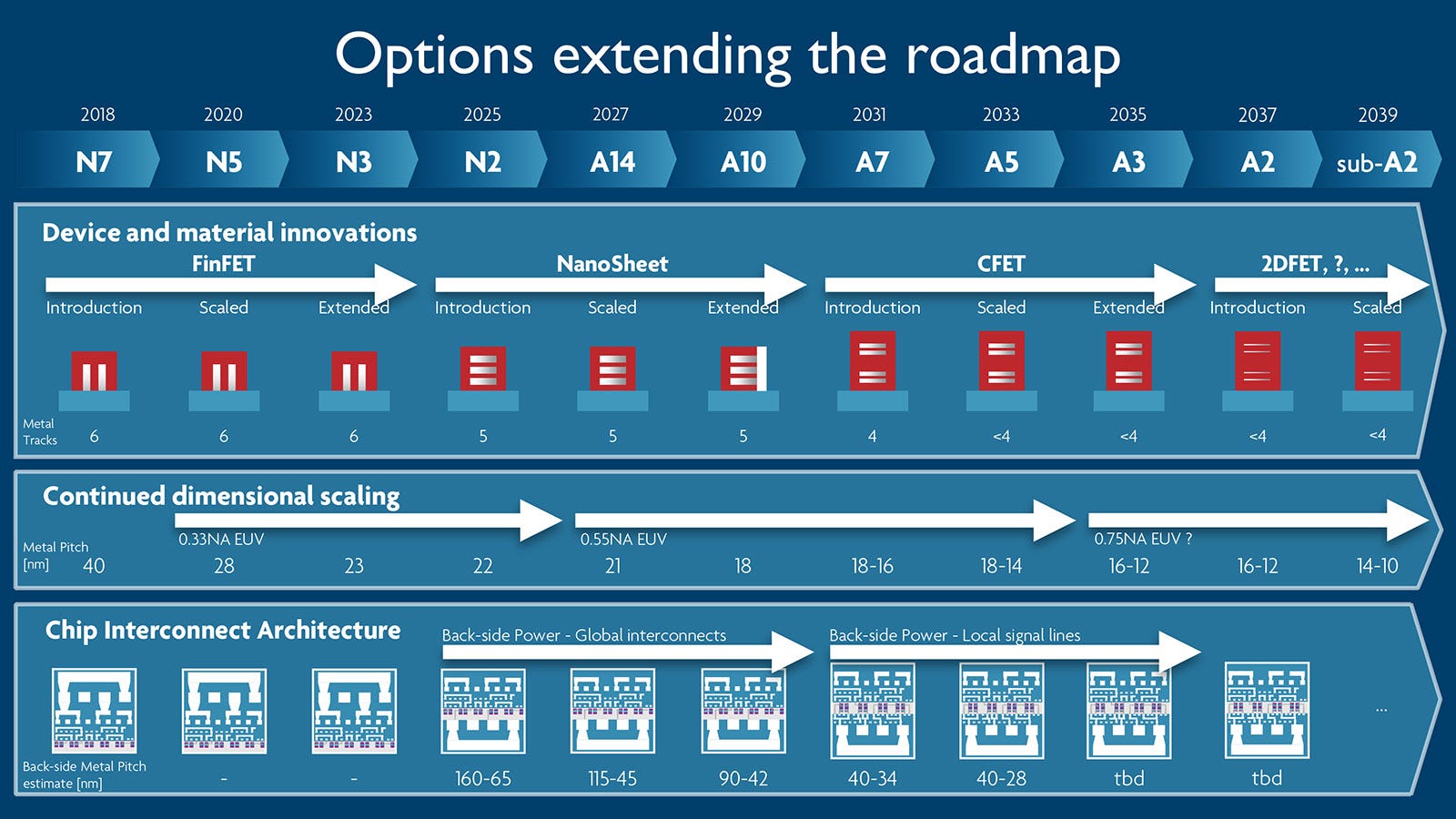
So why is Intel running it on 18A (its N2 equivalent)? 18A was designed around Low-NA EUV and multi-patterning, and the hardware Intel designed for it does not depend on High-NA to ship. Part of the difficulty of any new technology is ensuring it at least matches what it is replacing, and that’s why the layers on Panther Lake are dual-qualified on both Low-NA and High-NA, rather than just High-NA required. Intel has threaded the machine into a node that would be fine without it, so that by the time 14A/10A arrives and High-NA becomes more of a necessity, its people and its process recipes have done their learning already. If an 18A wafer went wrong, it’s not a big deal for the products until it gets dialed in – and Intel is now saying it’s dialed in.
People who follow Intel will understand that this is the reverse of the last transition, when Intel dragged its feet on EUV in the 10nm era and paid for the caution with years of delay. This time it is the one out front, and TSMC is the one waiting.
The cost argument that Intel ignored
The fair question is whether any of this is worth the money, and the skeptical answer comes from SemiAnalysis. Coming from IBM’s work on High-NA at a 2025 conference, they explain that a single High-NA exposure costs about two and a half times a Low-NA one. At that ratio, the new tool only pays when that one shot replaces enough cheaper ones. SemiAnalysis’ modeling put the crossover for most layers somewhere around 2030, with Low-NA double-patterning cheaper until a pattern needs three masks or more.
From a physics perspective, another factor is dose. To get the smallest layers, you need more EUV power, aka a higher dose, but a higher dose forces the scanner to dwell longer on each field. A slower scanner prints fewer wafers an hour, which pushes cost per wafer back up. TSMC has read the same math conservatively, skipping High-NA for its 2nm and A16 nodes and still being relatively non-committal through 2029, despite purchasing machines for testing.
What the bear case tends to underweight is that none of this has kept the machine from selling. ASML had ten to twenty High-NA orders booked by early 2024, and not only from Intel: SK hynix ordered too, and became the first memory maker to install a commercial system in late 2025. Samsung is also working with the tool(s) they’ve ordered. Even NY state has ordered one, being installed in Albany – to be primarily leased to IBM. ASML is building something like twelve to fifteen systems a year now and has guided to roughly twenty a year by 2028.
The objection regarding throughput and wafers per hour is being solved as well. The tool I saw back in 2024 was an EXE:5000 model, built for R&D volumes. The production EXE:5200B that Intel accepted at D1X in late 2025 runs about 175 wafers an hour at 0.7 nm overlay, a lift of roughly 60 percent, and ASML’s larger 6-by-12-inch mask is meant to cut the stitching overhead the halved field imposes. IBM in their paper also put up SPIE overlay data they argued showed no meaningful penalty from stitching.
The two sides are not really disputing arithmetic. Many analysts are trying to count the dollars per exposure. The foundries using the tool are also counting the exposures, masks, alignment steps, and defects they no longer have by only running once, not multi-patterning. Panther Lake is the first shipping evidence in that argument, and a matched-yield result is a strong point for the side that says the tool is ready to work.
Will I Ever Know?
No. I asked if Intel plans to SKU the High-NA parts differently so you could rock up at the office with a High-NA chip to gloat, but alas it looks like the hardware will just be run-of-the-mill parts bundled into the rest of them. I’m sure Intel will still be tracking by batch the long-term effects just in case, but the public will just get a CPU.
With Intel’s financials for the quarter quickly approaching, I can imagine some of the analysts on the call will be asking for volumes so far. I suspect it will fluctuate based on R&D uses for these tools, then when idle just pump a few Panther Lake wafers through to amortize some of the cost. In my first trip to D1X, I remember seeing a row of five Low-NA EUV machines all up and running, with at least a dozen more set for the facility as a whole. That’s how a foundry gets volume, so keeping track of Intel’s High-NA orders might be a good indicator for how confident they are long term about yield, quality, and cost.
Intel have already said that for external customers on 14A, High-NA will be an option – take it and you’ll have a faster time to market due to fewer steps, likely at an additional cost for next-day or two-day shipping.
