
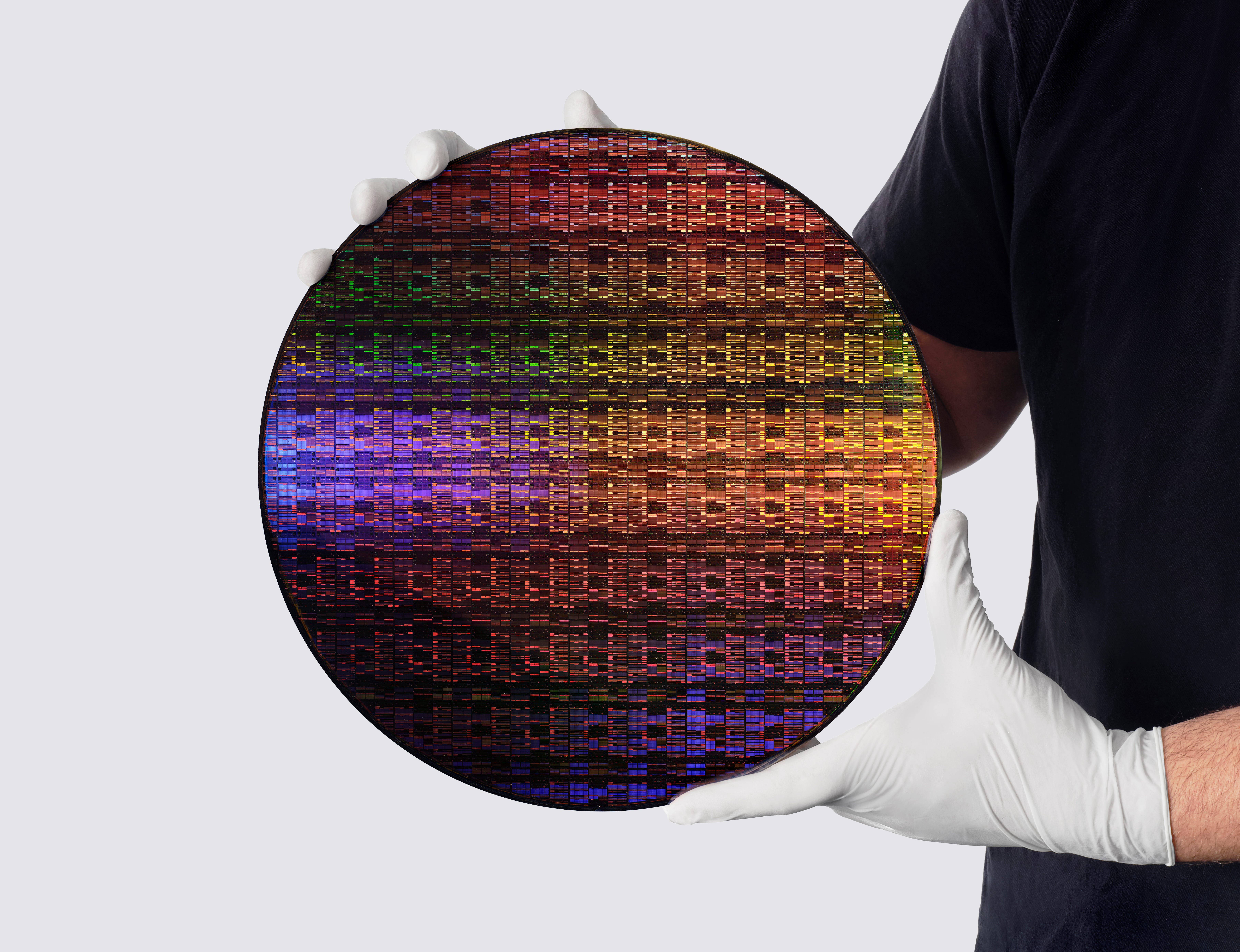
This is one of our classic deep dives here at More Than Moore that we’ve made free for all our readers. If you find this work useful, please consider subscribing to the substack at any level you feel comfortable and sharing the content. Or if you prefer video, you can find our podcast and other videos over at our YouTube channel. Thank you to all who are already subscribed, it really means a lot! 💖
There’s a reason why I keep asking high-profile executives and architects at major semiconductor companies about whether they think Moore’s Law, the process of improving transistor density*, is still in the works. On the one hand we’ve got Jensen at NVIDIA saying that Moore’s Law is dead, joined in part by Huawei but only simply because of not having access to the latest tools. On the other are AMD and Intel who recognise that Moore’s Law is part of the ongoing evolution and still remains a critical part. In the middle is TSMC, who in the words of Deputy Co-COO Kevin Zhang, told me ‘I don’t care.’ So who is correct?
When it comes to IBM, I firmly believe they’re in the camp of saying Moore’s Law is still alive. Four years ago, in 2021, the company announced it was the first to achieve a scaled Gate-All-Around (GAA) transistor design in a number of test vehicles between full logic and memory designs. This was substantial, as Gate-All-Around technology had been earmarked as the next stage beyond the FinFET designs that are common in the industry since 2012. IBM referenced the technology as a ‘2nm-class’ design, and while the only direct licensee of its technology is Rapidus in Japan, it paved the way for a wealth of Gate-All-Around designs to start hitting the market this year, in fact. While TSMC, Intel, and Samsung developed their own equivalents, IBM was proud to announce itself as the first.
Fast forward to 2026, and IBM is set to do it again. The transistor roadmaps from the leading research houses (eg imec) have earmarked that beyond several generations of FinFET then several generations of Gate-All-Around designs, the industry would pivot to a new design called CFET, or Complimentary FET. Instead of scaling transistors across a chip in a two dimensional way, CFETs enable a form of stacking, enabling more transistors in the x/y plane. There are multiple types of CFET design in the literature, and specifically IBM has built a staggered sequential CFET design. More on that later in the article.
IBM has dubbed its new technology with a marketing term: NanoStack. The baseline numbers look kind of mindboggling, similar to what we saw with the move from FinFET to GAA.
-
50% Logic Area Scaling
-
50% Performance at iso-power
-
70% Efficiency at iso-performance
-
40% SRAM scaling
-
666 Million Transistors per Square Millimeter (666 MTr/mm2) *
In these numbers, IBM is compared to its own 2nm process technology.
*The 666 number comes from IBM’s press release that states ‘100 billion transistors in the size of a fingernail’. IBM said half that number in a fingernail for its previous 2nm, and we got clarification they meant approx 150mm2. So 100 BTr / 150 mm2 = 666.66 MTr/mm2. There’s a better number later in the article.
IBM expects the scaling of the process to take around five years before this technology hits the market. IBM stated that the ‘expected markets who can take benefit’ of the technology would likely adopt it first, and based on current macroeconomics and chip design methodology, that’s still likely to be smartphone or small AI chiplets.
The company also states that this technology would benefit from High-NA EUV to reduce the number of patterning steps on critical layers. However it should be noted that it isn’t technically needed – IBM is currently in the process of installing their High-NA EUV tool and all this work was done without it. Oh, and IBM also casually/accidentally mentioned they bought a High-NA EUV tool.
In the rest of this article, we’ll go into the details we know about the technology, as well as some pre-amble to ensure we’re all on the right level.
The Transistor Roadmap
One of the best ways to understand what’s coming down the pipeline from the big players in terms of transistor design is to look at what’s happening in the research conferences and from the research institutions. Over the last decade leading up to the productization of the latest transistor technology, there are lots of research papers and presentations about work being done to build and develop what’s in the roadmap. What is in the roadmap? Well it up to now the transistors have gone through this.
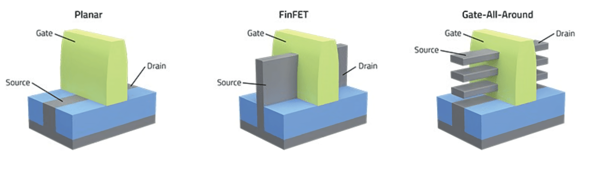
On the left is the Planar transistor, which was the main method for building transistors all the way up until the 2010s. It still is the base design for all chips built at 22nm and above, and is comparatively the simplest design, however it is the reason for a lot of advancements in this space. As we shrink a planar transistor to fit more on a chip, if we shrink them too much then the source and drain become too close causing electrons to leak, and the design reaching electrostatic limits as they shrank.
The FinFET transistor in the middle solved that issue. By extracting the source and drain up out of the substrate and wrapping the gate around it, this lead to better electrostatic control and conducting channels on three sides, rather than just the one. This leads to an increase in drive current for higher performance. Multiple generations of FinFET shrank the design but increased the height of the fins, to maintain balance. As scaling continues, tall fins become fragile to manufacture and the ‘fourth’ side of the fin without a gate is overpowered by the electric field. Not only that, but another way to increase density was through fin depopulation, using only one or two fins per transistor, which reduces drive current and switching speed.
This led to the Gate-All-Around design. By wrapping the gate all the way around the channel, the result is better control and current flow. Instead of ‘fin depopulation’, designers can control the number of layers in their gate, as well as the gate width, in order to fine tune the performance and power needed for a given cell or cell library. The complexity of gate-all-around comes from the need to build the layers or ‘sheets’ – while they look simple enough in this diagram, each one needs to be surrounded by a protective layer, and the steps to do that rely on some interesting chemistry and physics. The sheets themselves may only be five nanometers thick (so, 15 atoms) with a few atoms of protective layer, but the sheets often vary between 20 and 40 nanometers in width.
In the design phase of Gate-All-Around, we saw a wild array of approaches from the main players and research houses. Firstly around getting it to work in the first place, then designs from 2 sheets up to 7 sheets, with the materials and spacing being fine tuned. The first GAA silicon is now currently on the market as of late 2025, with:
-
Intel is using a four layer design branded ‘RibbonFET’ in its 18A process node technology (Clearwater Forest, Panther Lake, Wildcat Lake).
-
TSMC is implementing GAA in its N2 node using three sheets, with the first product expected to hit the market later this year with AMD and its new CPU, Venice (more on that at the end of August at their AI day).
-
Samsung would argue they were the first to market with GAA in their 3nm design process SF3E in 2022, with a crypto ASIC for MicroBT. Their first mainstream product with GAA on SF2 was the Exynos 2600 mobile processor in late 2025.
-
Rapidus has licensed IBM’s technology design and is currently installing tools in its new 2nm fab in Chitose, Hokkaido. It has already started running test wafers since 2025, with first product tapeouts in late 2026 and production ramp through 2027.
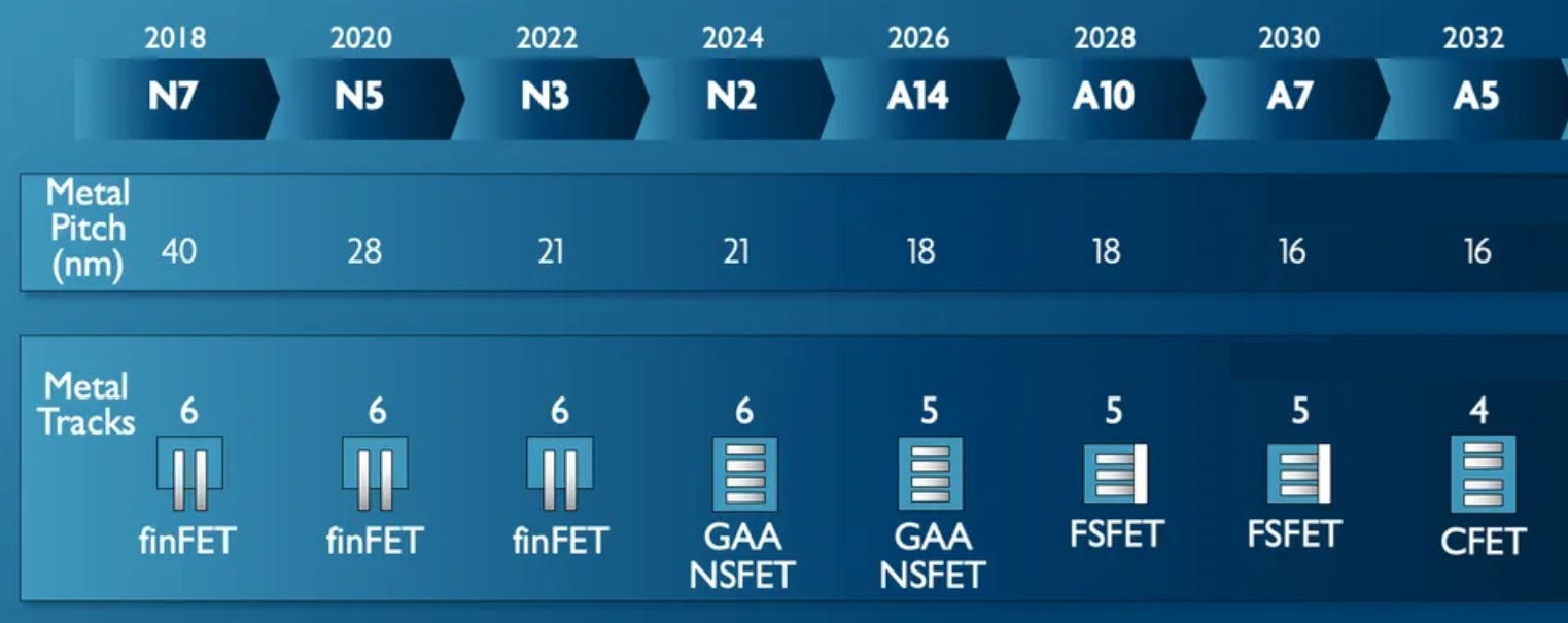
Here is imec’s roadmap from 2023. The process node names are a little behind, but it represents a key feature of modern semiconductor technology development.
From N7 to N3, imec highlights three generations of FinFET technology, with one of the main dimensions being metal pitch scaling.
From N3 to N2, we have the transition from the latest generation FinFET to the first generation of Gate-All-Around with nanosheets.
N2, A14, A10 and A7 are all generations of Gate-All-Around design. When we hit A10 in this roadmap, the gap between consecutive NFET and PFET gets replaced by a barrier to enable them to be closer together – this has been dubbed ‘ForkSheet’ in the literature but most players now just call it an updated version of GAA. Then we move into CFETs.
The point here is to show that each fundamental transistor design is built with several generations in mind, allowing for low hanging fruit improvements before a big pivot to something potentially a lot harder, with a lot more steps, or simply because the research hasn’t been done or the material science needs to happen. It takes a long time to do any of these steps, and hundreds of thousands of people. Not only the transistors but power delivery, metal stack design, and everything else.
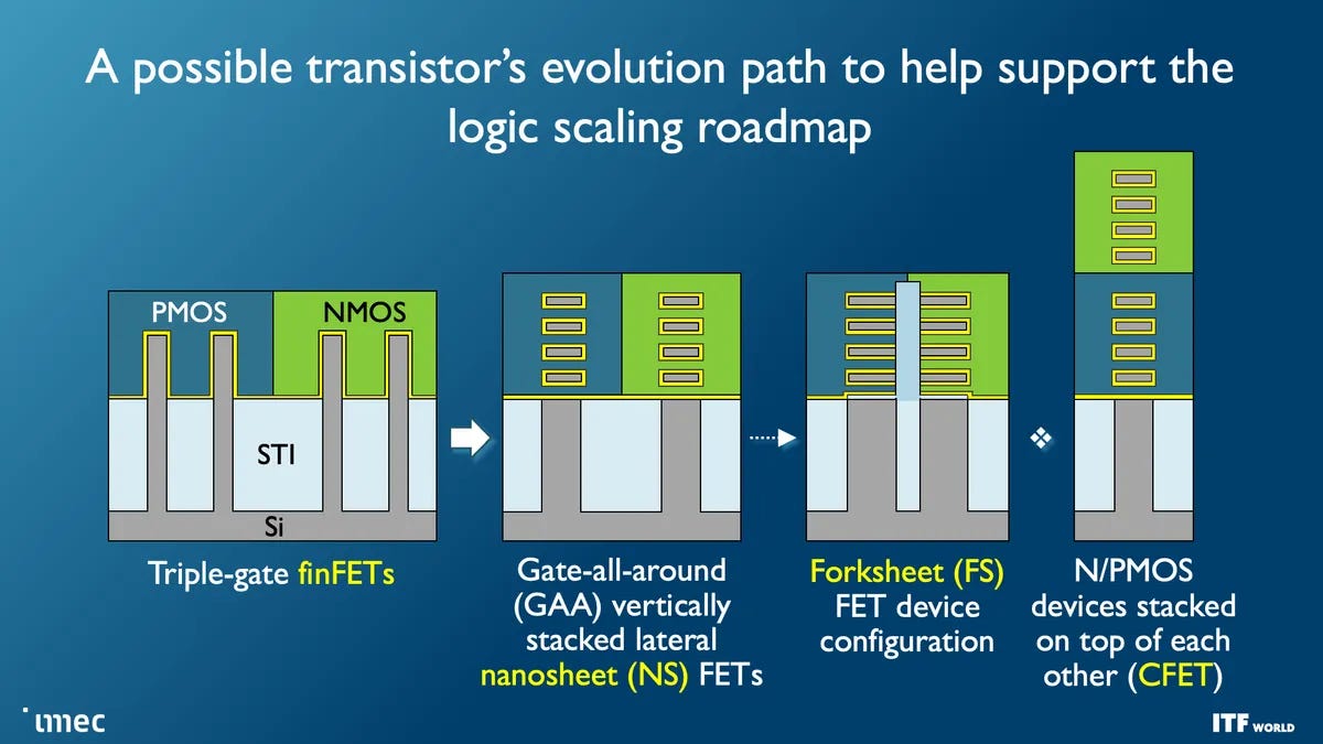
It means that when I show this image above, each one of these steps can be seen as a multi-generational effort, and not simply one after the other. CFET also comes in a variety of designs, has its own multi-generational effort, eventually leading to 2D transistors using Transition Metal Dichalcogenides (TMDs) like molybdenum disulphide (MoS2) and tungsten diselenide (WSe2). We’re expecting that announcement in 2031. That was a joke.
CFETs Normally Come in Two Flavours
On the face of it, given the image above, a CFET looks like a silicon designer’s dream. Overnight, it’s an immediate doubling of density compared to GAA. IMMEDIATE. I mean, look at that diagram – since whenever has a diagram been misleading?
Let’s start by mentioning at least some of the research that has led up to CFET. Technically by the definition of NMOS over PMOS as in the diagram, it’s not always necessary that the two parts have to be GAA, i.e. GAA on GAA. Over the last five years we’ve seen research from Intel and others showing one Fin on one sheet of GAA, Fin on Fin, and maybe even planar in the mix. That’s simply because planar and fin are well known processes. A lot of this research was also done at larger nodes too.
However in the last 3 years or so, we’ve seen more efforts for two-sheet GAA on top of two-sheet GAA, and the evolution of that. Ultimately production level CFETs are expected to be 3-on-3 or 4-on-4 or a mix in between.
But truth be told, there are two main ways that the industry has been looking at even building these designs. We call them monolithic CFET and sequential CFET.
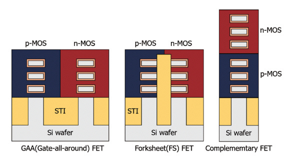
Monolithic CFETs (mCFET) have a clue in the name. Much like a multi-sheet GAA design, a monolithic CFET will build all six to eight layers on one piece of silicon, then do the etching/plating/filling as necessary. There’s some additional control needed to enable that, but broadly speaking it’s as complex as building more layers onto a GAA design. The top line benefits of such an approach are meant to be simplicity and density.
A lot of work is being placed into mCFETs to ensure performance, yield, and scale. One of the main issues is the restriction on process steps as the stack is built higher. Because pMOS and nMOS have different materials that build them, any step to build the nMOS on top of the pMOS (and vice versa) cannot interfere with what is underneath. So you can forget that 1400ºC annealing step and spend years trying to research a new way that is as good, as cheap, and as scalable.
Sequential CFETs (sCFET) instead bond together using two or more wafers. That’s a relatively easy way of looking at it, but there are multiple methods.
-
One, each wafer has a set of GAA devices on them, either all nMOS or all pMOS, and with some clever physics, are bonded together such that they connect in the right places with the right overlay and act like a CMOS transistor pair. The benefit of such a design means that each type of transistor can be heavily optimized without worrying about the effect on the other – even more so than a traditional GAA or FinFET design.
-
Two, the first wafer has a set of GAA devices on them, and the second carrier wafer brings over some structures for the upper tier and the rest of the design is fabricated on top. This is a stop gap to assist with specific device optimisation, but still needs careful planning to deal with thermal integration as mentioned above.
The downside is the bonding – it has capacitance and a margin of error, and any slight deviation makes both a lot worse.
There’s an interesting discussion as to which process might be more expensive. On the one hand, mono-CFETs have additional layers on the same wafer, leading to cascading yield metrics on a single piece of silicon. By contrast, sCFETs can only need half the number of sheets on each wafer, but the cost comes from the bonding accuracy and yield loss. In the diagram above, imec is showing three generations of sCFETs and how the bonding between them evolves.
Which one of the two is better is hard to say, and will depend long term based on the research. Again, if we’re looking at 2031 for the first CFET designs to hit the market (we still have 3-4 generations of GAA first), then how those designs are improved and research will determine which ends up better. An old report from SemiAnalysis in 2024 claimed that all the leading fabs were primarily looking at mCFETs.
IBM’s CFETs Are Wonky By Design: Part 1
Instead, IBM is going down a third route.
It has been known for a while that NMOS and PMOS transistors prefer different orientations of silicon atoms. If you’re wondering how silicon has different orientations, it’s all to do with the lattice inside and if you were to cut it in a specific direction, where exactly you would cut it.
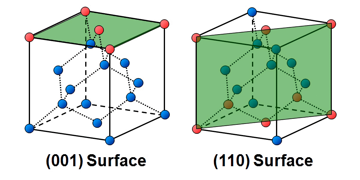
The green lines are where you would cut an infinitely repeating crystal. So on the left, a cut into silicon in the (001) plane would give you five atoms in red direct, whereas in the (110) would give you eight atoms in red. You can cut in any plane, such as (010) or (101) or (011), but these are the two that matter in this context.
It turns out that for transistor performance, NMOS transistors prefer (001), and PMOS prefer (110). What this means is the “mobility of the conducting element” in each transistor type is improved by the different silicon orientation. If you’re also wondering why I worded it that way and didn’t simply say mobility of electrons, it’s because NMOS uses electrons but PMOS uses electron holes. It’s a material science thing that works, and the mobility of each matters, but is beyond the scope of this article.
The problem with needing two different silicon orientations is that in a monolithic design, you are limited to one or the other, at least in planar and FinFET transistors. You could technically grow silicon epitaxially in the right orientation in the right spots, but it’s often difficult, time consuming, expensive. As a result, most wafers prioritize the NMOS transistors, hoping the PMOS performance is up to par. Over the years, additional strain to the channel has also been created artificially to improve performance. In FinFETs, because there’s an additional side in the design, technically the channel is exposed on two planes, which can be beneficial.
In Gate-All-Around designs, you also have two planes, except now the sheets are long rather than tall, emphasising the (100) plane loved by NMOS. Again, strain is also added through the silicon-germanium liners around the sheets to improve performance.
In sequential CFETs, there’s now an opportunity to use two different wafers with two different lattice orientations. This is one part of what IBM is doing.
The manufacturing process looks as follows:
-
Build PFETs on carrier wafer with (110) channel
-
Use 2nd carrier wafer to bond on the top layers of silicon with (001) channel
-
Remove 2nd carrier wafer
-
Use new (001) silicon to build NFETs and backside integration***
-
Attach new 3rd carrier wafer
-
Flip over and detach original carrier wafer
-
Build backside integration on original PFETs
It looks a little like this:
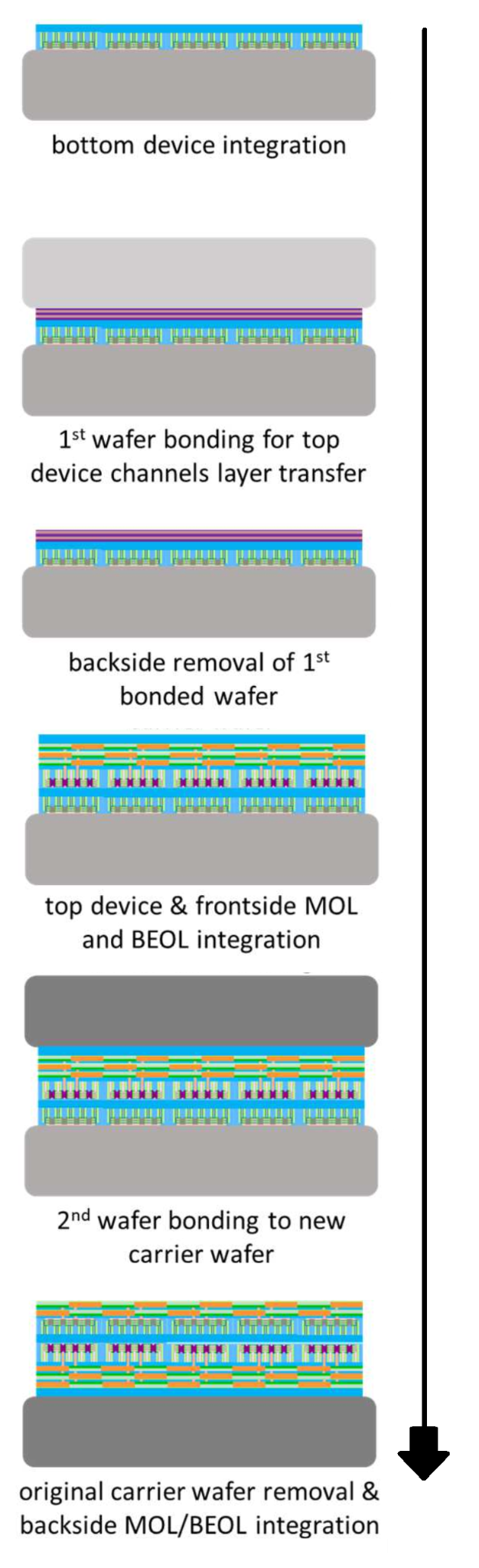
Now for those of you following closely, there’s a triple asterisk in my list above and in the image. This is important, because here IBM is building the top layer of transistors in the new crystal structure. This means we have what looks like the same issues as with monolithic CFETs – one wrong high-temperature process step and the whole thing goes kaput.
IBM says they managed to solve this by using techniques inspired by 2012 gate-first High-K Metal Gate technologies to the NFETs with replacement metal gates, the problems are resolved. They showed this graph.
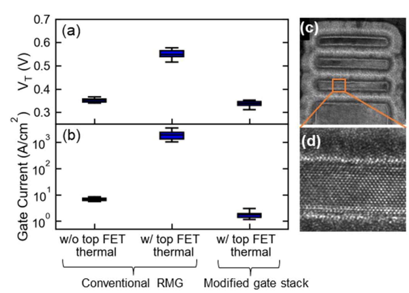
With conventional replacement gate methods on monolithic designs, the two numbers on the left show the effect of the thermal issues. We see here the damage it does: the threshold voltage (Vt) increases from 0.35 to 0.55 volts, and the gate current/leakage goes up by two orders of magnitude. Sometimes this is likened to a leaky faucet, but instead of a drip you end up sailing down the street.
On the right are IBMs results in solving the thermal issues in their stack – an almost similar threshold voltage (which looks pretty damn good), and an even better gate leakage.
But in short, for Part 1 of IBM CFETs Are Wonky, it’s because they use two different crystal lattice directions in a sequential CFET design.
IBM’s CFETs Are Wonky By Design: Part 2
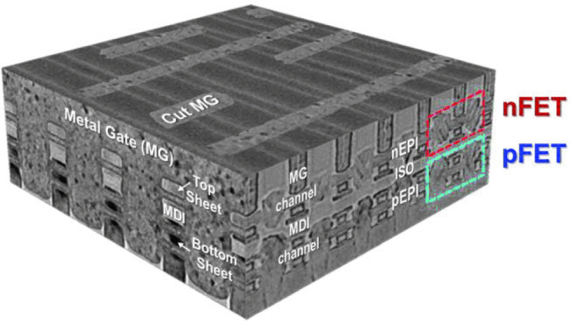
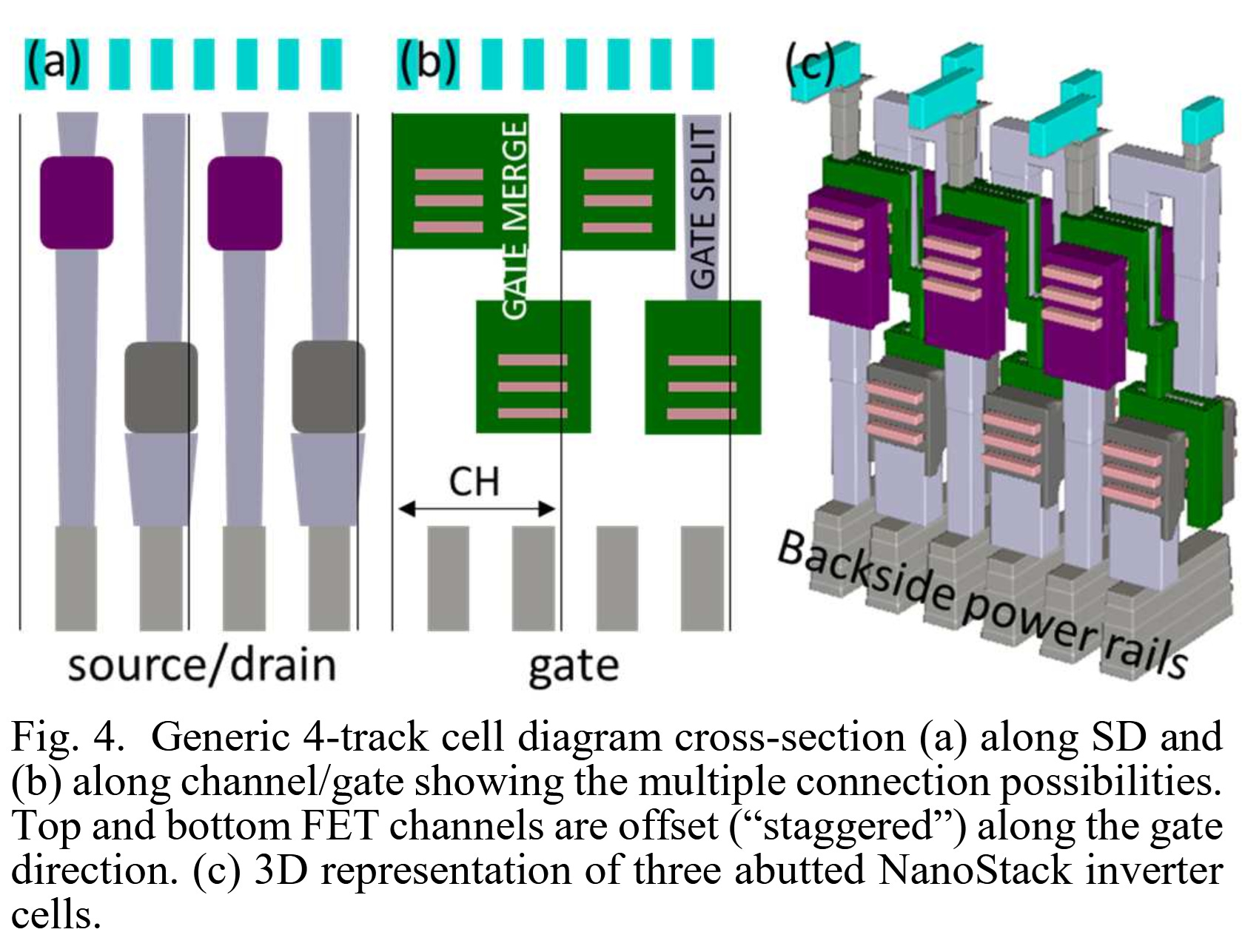
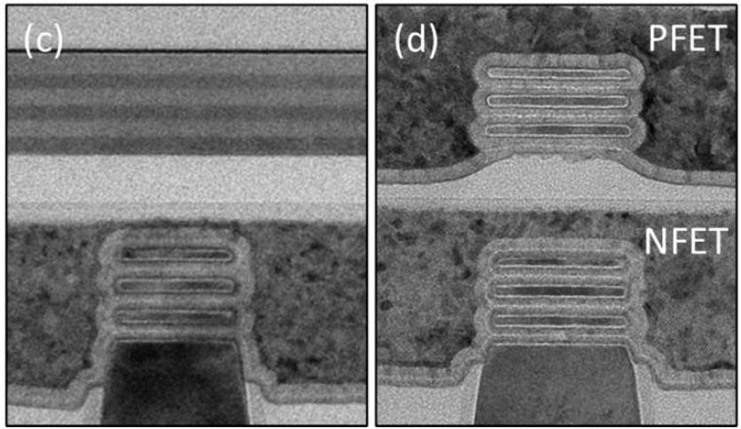
In their research, one of the critical limiting factors in CFET design is where you put the channel contacts. A regular CFET image doesn’t really show it that well, but both sides of the transistor need contacts for power and signal in order to work. In a purely stacked linear design, that has issues.
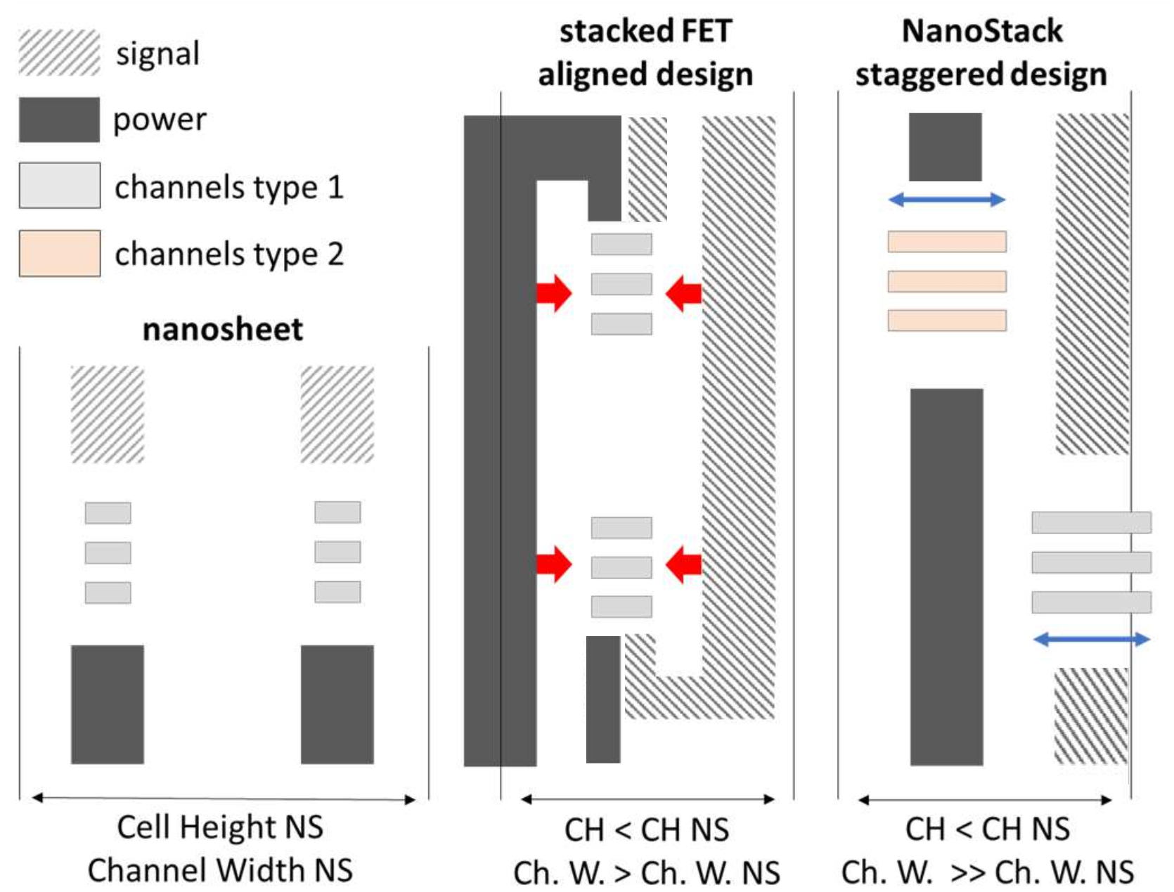
In this diagram, on the left, we have our three-sheet GAA transistors, each with signal and a form of backside power. That’s how some of them look today with GAA designs on the market.
In the middle is what happens when there’s a stacked design. Due to the signal and power coming in from the opposite side for each transistor and having to circle around the other part, there ends up being a lot more signalling and power to deal with. Also, due to those additional connections, the width of the sheets in a sCFET have to shrink and are limited in size.
On the right is what IBM is doing. They claim it to be a unique approach in the industry – a staggered sCFET design they’re calling NanoStack. By offsetting the NMOS and PMOS from each other, it allows for direct connectivity from either direction. This not only makes it easier to design, but allows for the sheets to have a wider range of effective widths, allowing for higher power and faster switching transistors for the target markets.
The key difference here is that diagrams of monolithic CFETs often leave out the connections on the transistors because they haven’t really been needed before when talking about density and drive current. This time however, IBM is claiming up to a 65% increase in effective gate width per 4-track cell compared to an ‘aligned’ sCFET design.
Here’s another nice image of the staggered design in their modelling software, showcasing the easier and more regular approach that the staggering allows.
The Secret Sauce: Bondage
In our briefings with IBM, they were keen to point out that this staggered sCFET design is only possible due to the unique bonding technique they have created, enabling the crystal lattice orientation changes. I’ve discussed at length on stage and on calls to clients about the differences in bonding technologies, but IBM says it’s doing something different and unique to enable this.
IBM is keeping the exact recipe a secret, but has given us hints. So I’m going to describe the problem, and what we do know. Let’s pull out a diagram that based on Huawei’s recent announcements has become popular again. It’s the 3D stacking scale diagram from AMD.
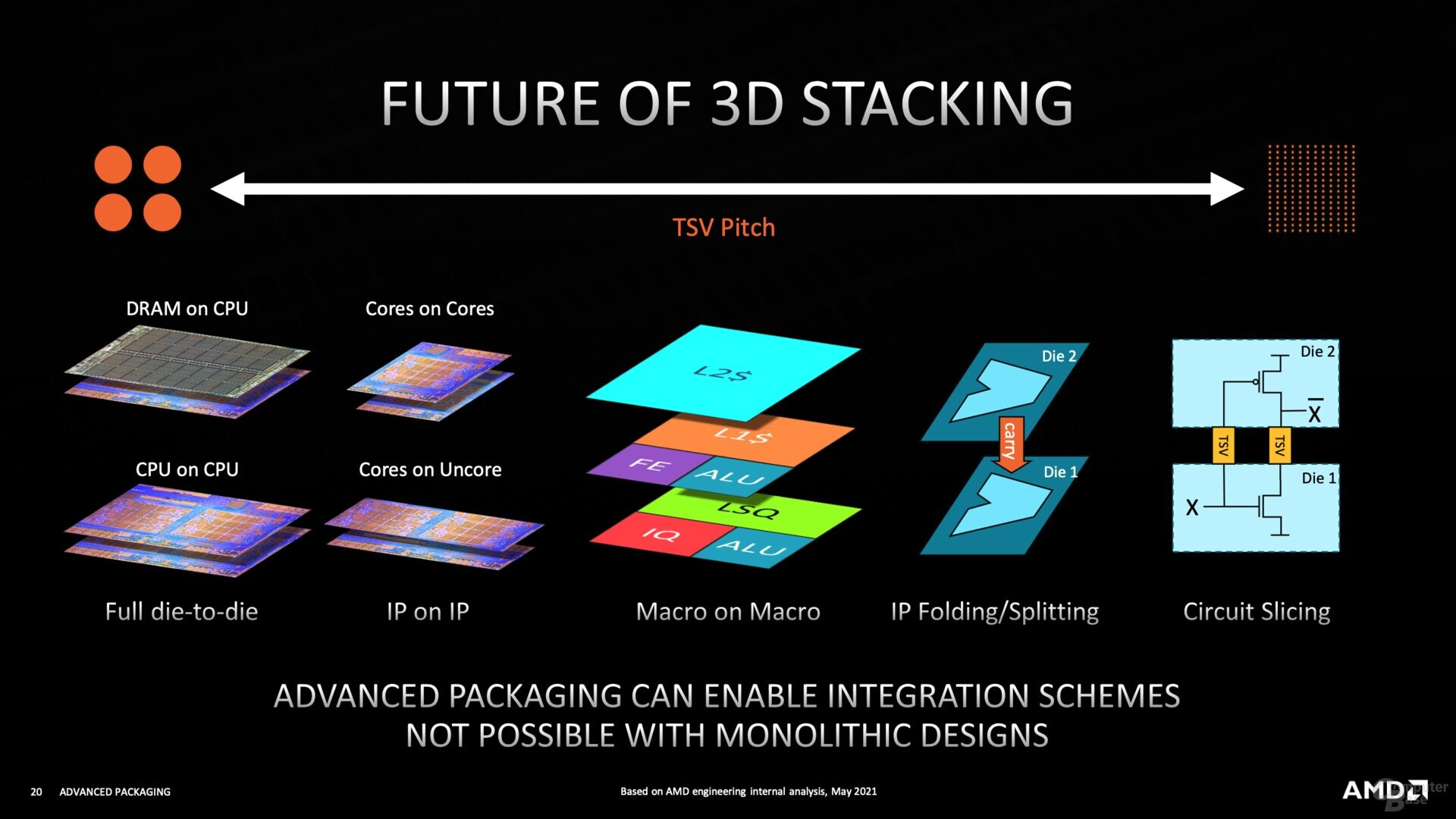
This diagram shows how tight the connection pitches need to be to enable different forms of stacking. The reason for this comes down to performance, power, and complexity. The closer to the silicon the sub-divisions of the design, the more connections you need, and thus the tighter packed they need to be. On the far left is traditional C4 bump bonding, with a bump-to-bump pitch around 50 microns, coming down to 35 nm using micro-solder balls, or 20 micron using copper pillars. Then we move to direct copper-to-copper bonding with hybrid integration on the right, going from 9 micron pitch down to 4, 3, or even 1 micron.
The thing is, even at that level we’re still only at the circuit splicing. Now, there’s a small definition problem here – what exactly would you call circuit splicing and how is it different to IP folding? Are we subdividing at the library level, the cell level, or something deeper? I tried to create something that evolved the original slide.
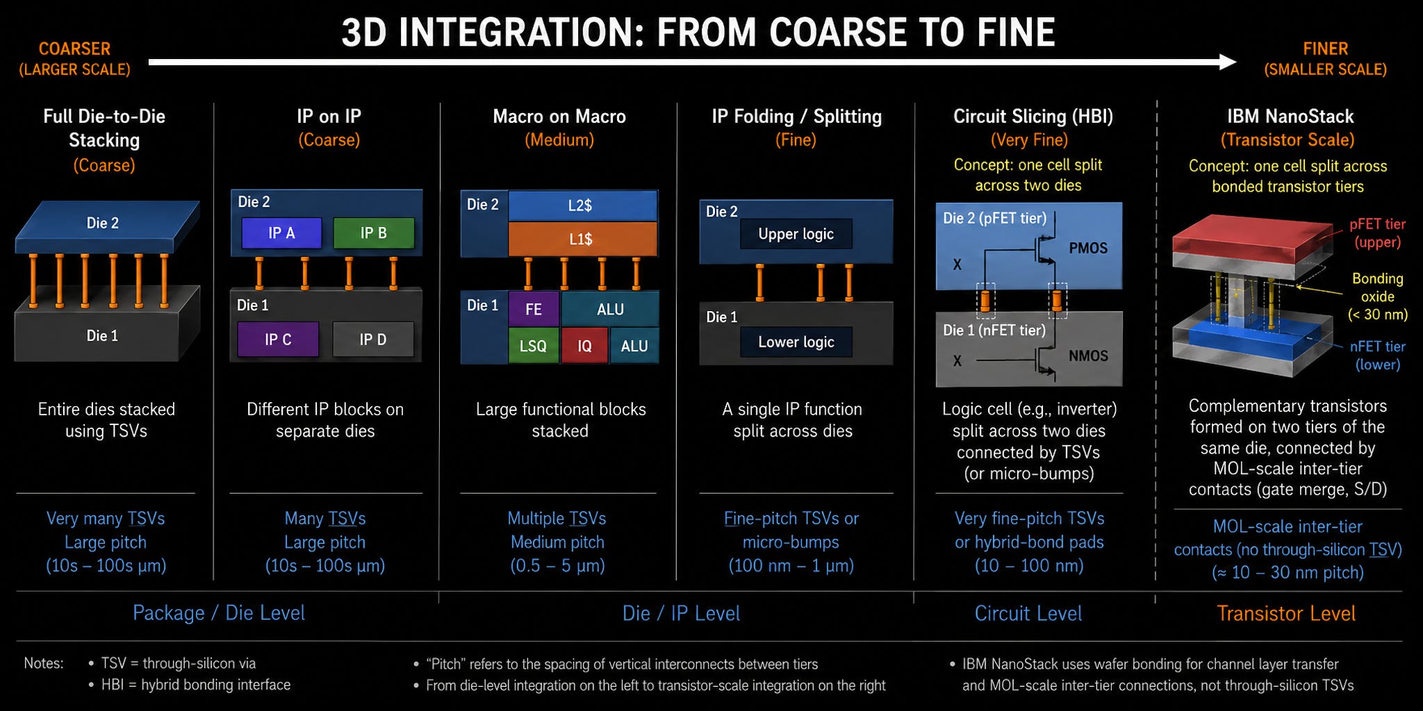
I actually went down a little bit of a rabbit hole on this one and got nerd sniped. The issue is that AMD’s original slide shows circuit slicing using TSVs, which are normally a back-end manufacturing process (done at the end). In order to make that work, it would actually be more like a ‘just before the true BEOL starts’.
IBM on the other hand describes its bonding process as categorically not back-end of line, with a completely different technology of doing it, enabling finer grained pitch contacts. This is because they build the NFETs into the silicon as it’s deposited, so the bond between the transistors isn’t as simple as a TSV shown in the circuit level splitting.
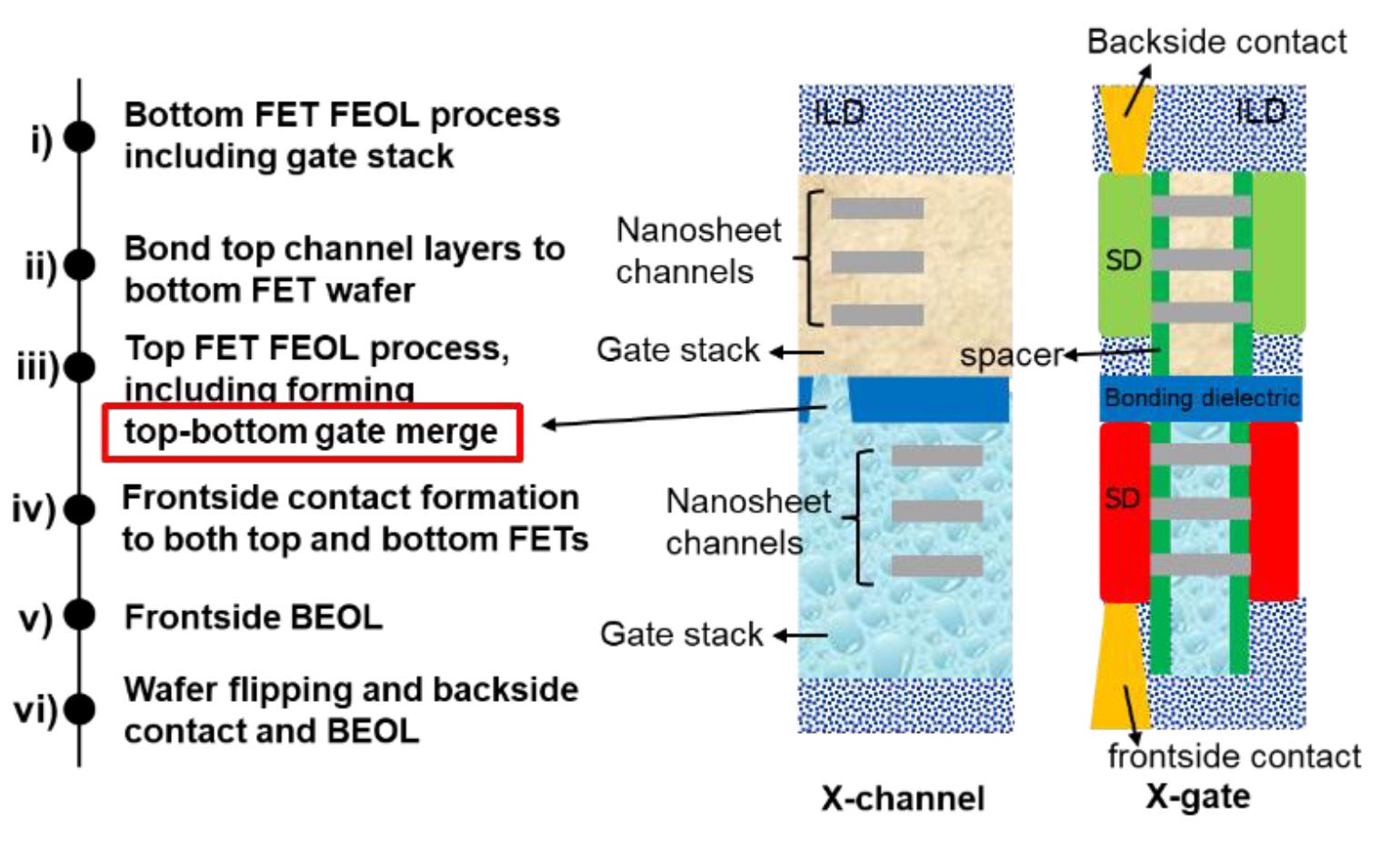
IBM calls what they’ve done a ‘gate merge’ design. They’re using a bonding dielectric during the front-end design process (i.e. at the start). This enables the bonding between the lower layer and upper layer to be defined before manufacturing of the top layer takes place, and thus metrics such as overlay don’t factor in like a TSV design. This is what makes us confident that IBM’s overall density numbers for transistors are more believable than Huawei’s simpler TSV IP splitting technology using older process nodes.
All that being said, IBM’s narrative in our meetings is that the bonding technology is what has enabled all of this, and that’s why it’s very special and very secret. They mention in the papers that 10 nanometers of bonding oxide equates to a 2.5% increase in cell-level effective capacitance, so reducing that as much as possible is a key dimension. At VLSI, IBM showed a sub-30 nm bonding layer, verified via scanning acoustic microscopy to be within 1.5 nanometers across a full 300 mm wafer.
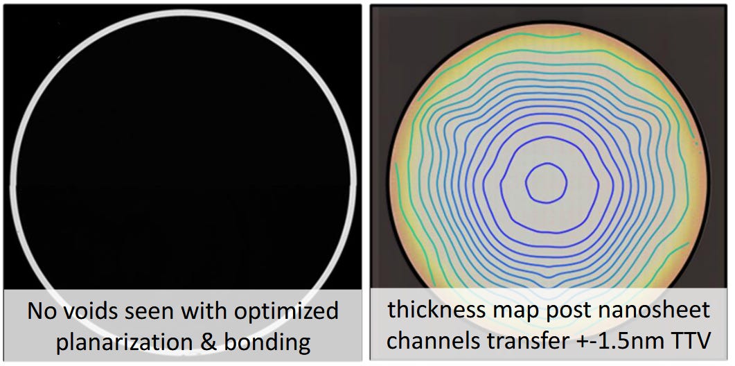
The end result is a set of crystal lattice layers on the top of the wafer ready to be built into. The following image shows after the bonding, and then after building the transistors.
The end result is a pair of transistors that don’t look out of place in any other design. Usually with transistor design, one of the main metrics is how current scales with applied voltage. The magic number for CMOS designs is always to get as close to 60 millivolts per decade (per order of magnitude of current) as possible, as the lower that number the easier it is to turn on and off the transistors.
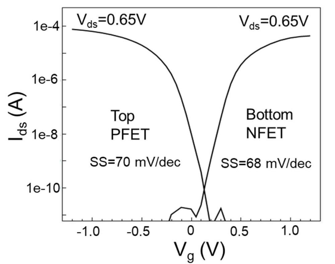
IBM scores 68-70 millivolts per decade, which considering the time from high volume manufacturing is really good. By comparison FinFETs can be from 65-85 mV/dec, and planar transistors are around 80-100 mV/dec. FD-SOI, a high-performance planar alternative, goes between 65-75 mV/dec. GAA is expected to be 60-75 mV/dec in its lifetime.
Numbers
Now let’s talk about some physical numbers when it comes to transistor cells. When designing a chip the designers work at the cell layout rather than the transistor layout.
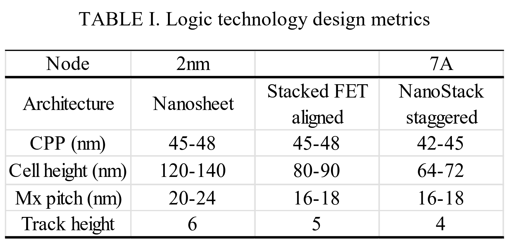
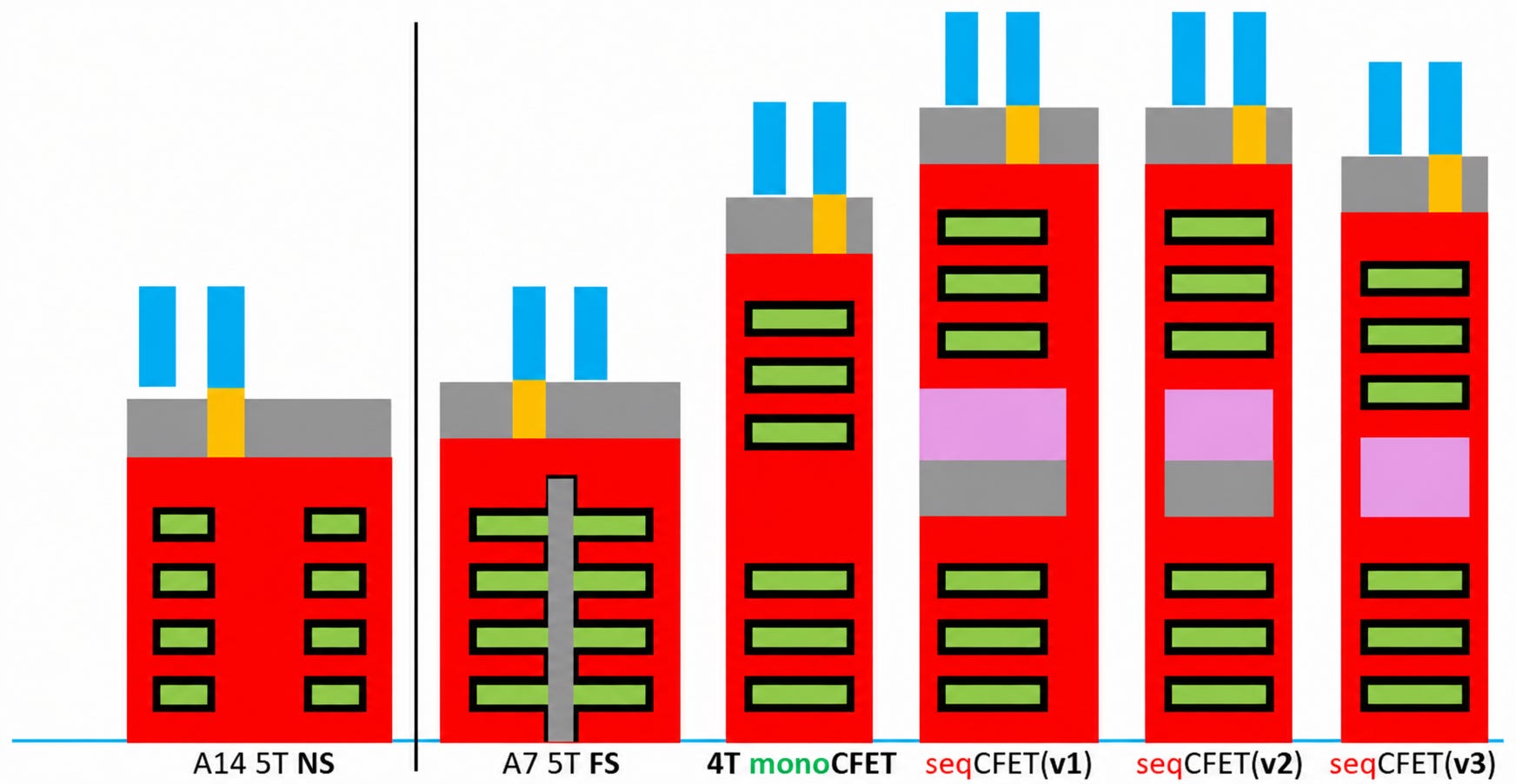
In this table we have IBM’s 2nm compared to their 7A Nanostack, with some aligned sCFET in the middle.
The major change is the 50% reduction in track height. In a cell design, tracks are built to support signal and and power connections – IBM believes a 4T design is most efficient with their sCFET. If we multiply the track height by the metal pitch, we get the cell eight numbers.
The area proxy for a standard cell is roughly CPP multiplied by the Cell Height. This gives us:
-
2nm GAA: 6045 nm2
-
Aligned sCFET: 3953 nm2 (35% reduction)
-
Nanostack sCFET: 2958 nm2 (51% reduction)
Relative to 2nm, this is where IBM’s 50% scaling comes from.
IBM also showed off this graph:
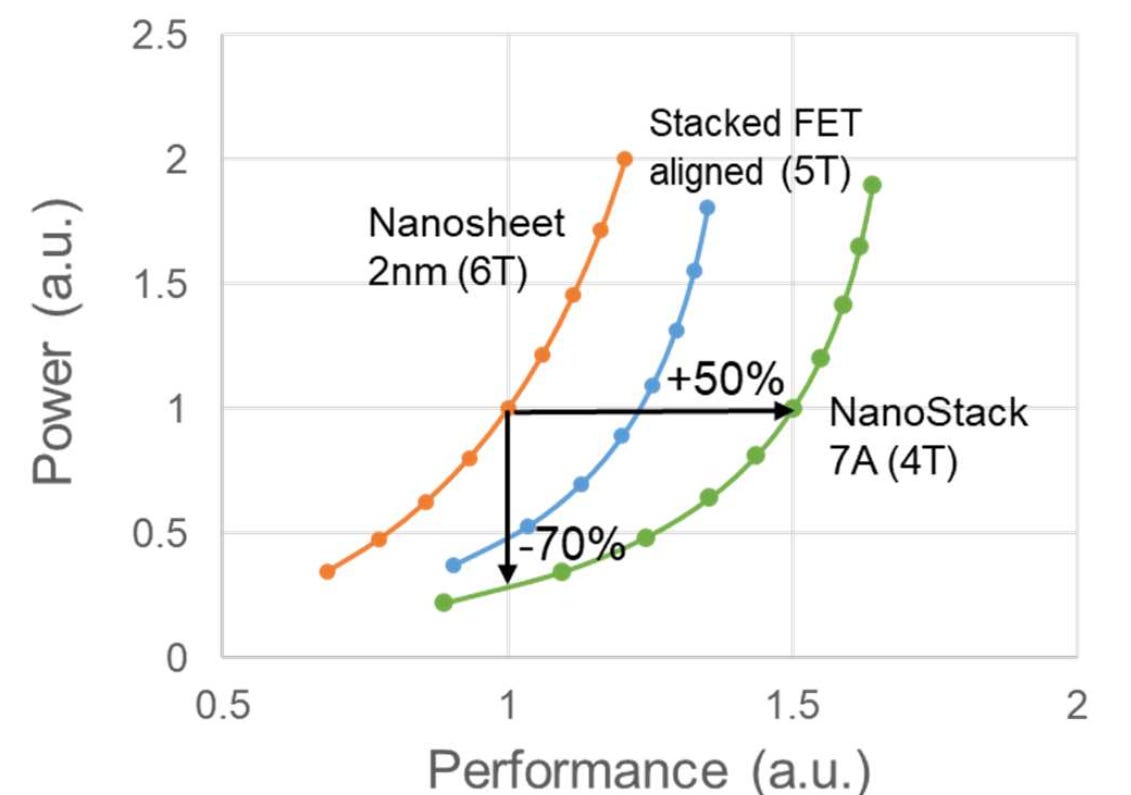
Unfortunately no detail was given as to how this graph is calculated, although it’s worth noting this is based on transistor level metrics, not cell level, IP-level, or chip-level designs.
To be honest, I think the most impressive line is if we look at the nanosheet (6T) peak performance. It’s at 1.2 AU but using 2 AU of power. We can draw a line straight down from that to NanoStack 7A.
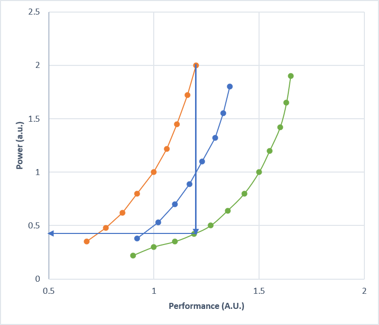
That’s down to a power of 0.42 AU. That’s a 79% saving. Insane.
Let’s talk SRAM Scaling
While technically most of IBM’s numbers here were published in their 2025 VLSI paper, it’s what came through the 2026 submissions that enables them to have this announcement today. One of the key limitations in transistor node scaling has been SRAM, and given the ratio of SRAM to logic on a modern processor, if it doesn’t shrink then the effect of a process node change means little to nothing. One of the prospects with CFET, given its literally stacking one transistor on top of another, means that with a perfect geometry we should see a doubling of SRAM cell density overnight. That naïve way of thinking is a good place to start, although with the additional periphery needed for SRAM control, IBM is claiming a more modest 40% reduction in cell height compared to its 2nm process. Still, nothing to be sniffed at.
Modern SRAM is compared by either cell area in square microns, or density in megabits per square millimeter – and it is usually built with the high-density process variant. Currently the leading numbers are:
-
TSMC N2: 0.0175 µm2, 38.1 Mb/mm2
-
Intel 18A: 0.0210 µm2, 38.1 Mb/mm2
-
Synopsys on TSMC N3: 0.0213 µm2, 38 Mb/mm2
-
Samsung SF3/2: 0.0199 µm2, 29.02 Mb/mm2
(data from ISSCC 2025, Kurnal Insights)
In IBM’s research, they found that the staggered sequential CFET approach actually allows them to tighten some of the transistor gate spacings for better density compared to the basic aligned approach.
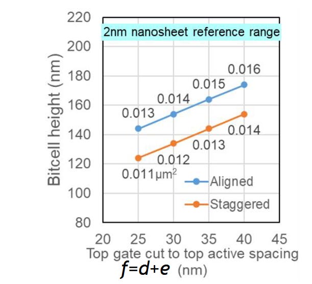
The y-axis on this graph is showing bitcell height, and the x-axis is a measure of how much they can push some of those spacings. On the face of it, the smallest bit cell is 0.011 µm2. That could yield a theoretical maximum SRAM density of 90.91 Mb/mm2, however real-world density is usually around 55-65% of this number, meaning a probably real-world density of just shy of 60.
-
IBM 7A NanoStack: 0.011 µm2, 54.5-59.1 Mb/mm2
On The Topic of Transistor Density
Now I’ve mentioned this once or twice before, but it’s important that it has its own section.
Historically transistor density, in its very name, should be measured by how many transistors you can fit into a given area. Since time immemorial (aka September 3, 1189), most protagonists in this space have assumed that value to mean on a singular piece of monolithic silicon, i.e. an x/y dimension limit.
Where this definition requires scrutiny is in the event of going vertical, i.e. stacking. This applies to multiple chiplets stacked together, as well as what IBM is doing with sCFETs.
To begin, I think we can agree that monolithic CFETs still fall under the original definition and are fine.
We typically do not sum up directly bonded chiplets and consider that a density increase – eg AMD’s V-cache or MI300X technologies. Each piece of silicon has its own density.
Huawei recently announced its Logic Scaling, which based on our graph would be IP folding. The company claimed that this was a density improvement, by layering cell libraries on top of one another using TSVs for more direct communication. I fundamentally disagreed, and said Huawei was extracting the urine on that one. I saw the reason why, but felt it was an attempt to pull the wool over the eyes of the general public. Given how successful commentators in this space still don’t realise that ‘3nm’ is a name and not a dimension, Huawei were hugely successful with their news. I guess that’s why those commentators get invited and sponsored by Huawei. But if we went down Huawei’s route, if I bonded five chips together at 50 billion transistors each at 100 mm2, suddenly I now have 250 billion in the same area. That’s not a node increase, that’s just urban planning.
The thing is, IBM’s not doing that. They’re still building transistors into the same piece of silicon. It’s just that what they’re building into was carried over and bonded onto the original transistors. The delineation is not through TSVs, but direct transistor-to-transistor connections that the method builds in, rather than traditional hybrid bonding. It’s within the cell library, rather than between cell libraries. To me that still counts.
So time for some math. For ease of use, I’m going to be using Kurnal Insights for some numbers.
Let’s use Intel’s/Bohr’s formula for calculating density. It uses the cell height and gate pitch to build up sizes of two of the most popular types of structures in a processor – NAND2 (memory) and Scan Flip Flop, SFF (logic). Then it uses a typical ratio of these to get the density numbers. There’s also a caveat about separating transistor regions, called diffusion breaks. Also high-performance designs will be different to high-density designs.
Huawei did a different calculation scheme. I could include those for fun.
Nonetheless, some numbers.
IBM Nanosheet 2nm
-
Cell Height: 120-140 nm
-
Gate Pitch: 45-48 nm
-
Density: 219.30 – 272.90 MTr/mm2 * (originally reported 333 MTr/mm2)
-
#HuaweiMath: 370.37 MTr/mm2
IBM NanoStack 7A
-
Cell Height: 64-72 nm
-
Gate Pitch: 42-45 nm
-
Density best case: 548.25 MTr/mm2
-
#HuaweiMath: 744.05 MTr/mm2
To put that into perspective, here are the high density numbers from current and popular process nodes.
-
Huawei 2031: 400+** using HuaweiMath
-
Huawei 2030: 292.00** using HuaweiMath
-
Huawei 2026: 238.00** using HuaweiMath
-
Rapidus 2HP HD: 237.31
-
TSMC N2 HD: 236.17
-
TSMC N3P uHD: 223.96
-
Samsung SF2 UHD: 206.11
-
Intel 18A HD: 184.24
-
Samsung 3GAP HD: 182.75
-
Huawei 2025: 155
-
Intel 3 HD: 140.35
-
Samsung 4LPP HDL 137.83
-
TSMC N5 HD: 137.60
-
TSMC N7 HD: 107.73
-
Samsung 7LPP HD: 102.28
-
Intel 10nm HD: 100.33
-
SMIC N+2 HD: 92.82
-
Samsung 8LPP: 60.92
-
TSMC 10FF: 55.92
-
Intel 14nm: 44.40
-
TSMC 12FFC: 39.98
-
GF 14LPP: 32.80
-
Intel 16nm: 21.26
Three trends stick out.
First, what are you smoking Huawei.
Second, IBM’s best case 2nm number from 2021 still hasn’t been achieved. That might be an indication of where sCFET gets to in a similar timeframe.
Third, IBM NanoStack 7A worst case is ~382 MTr/mm2. That’s if you use the worst case dimensions and need a double diffusion break between cells. But if you take either number, it’s still a sizeable jump.
The Other Parts of the Puzzle
Between two papers, two sets of slides, and the equivalent of a few hours of questions in my hands, this is the article. There are a few more points to flesh out due to the answers of those questions that don’t really fit in anywhere. So they’re going here.
Q: What is the minimum threshold voltage? One paper shows a test at Vds of 650 millivolts, and the thermal testing shows Vt at around 350 millivolts
Answer: it’s similar to a scaled version of 2nm
Q: What material is the gate-merge interface material? Does it follow IBM’s research with Tungsten and Titanium Nitride liners as via contacts?
Answer: Cannot disclose at this time.
Q: Is IBM still researching monolithic CFETs? I know many factors go into this, like physics or economics, but in your personal opinion, what would you think has more scaling potential – monolithic CFET or staggered/sequential CFET?
Answer: IBM started on mCFET first, we called it 3DSFET back in 2014. We spend 3+ years understanding the constraints. However we developed the staggered design when we understood it offers flexibility.
The additional thing is that you stack more layers with this staggered design. Once you build signal lines and power lines into each wafer, it’s stackable, unlike mCFET. sCFET enables z-direction. Fully leveraging z-direction for transistor scaling.
Ian: Once you solve for thermals, daaaaang. IBM has a bunch of patents on that from the early 2000s. It will be interesting to see where it makes sense compared to chiplets though.
Q: The images on the slides are showing approximately 60nm gate width. Normally we see 20-40 nanometers with current gate-all-around designs. Is 60nm indicative or just representative?
Answer: When the sheet is wider, if you can fit into the density, and the performance is better. That limit in a nanosheet is by device but also due to CMOS patterning on the device stack. There are also NFET vs PFET differences. With sequential CFETs, you can do that independently compared to CFET which has to stay the same. As we’re also not limited by NFET vs PFET differences, it increases the margins in the sheet width for better optimization.
Q: Do staggered sequential CFETs have direct benefits with defect yield? A follow up – is it even possible to test the different NFET and PFETs before bonding to ensure working transistors?
Answer: We haven’t really practiced that – there are concerns with introducing tests into the manufacturing process. It took us a year to model and develop the thin dielectric bonding – but we test for thin dielectric with no wafer distortion so it’s defect free. But for testing we are looking at the idea.
Q: How do you think NanoStack would change the EDA approach to circuit design?
Answer: We’ve said that it will take 5+ years to bring this technology volume. That covers all aspects – the technology, supply chain, but also the EDA. It is time for EDA to embrace the vertical direction – it’s similar to EDA in 3DIC at the chip level, but this is the first time enabling 3D at transistor level, and EDA enablement in the next few years is critical. We also need to work with our tools partners to deal with metrology and inspection in 3D.
Q: What thermal, signal integrity, and power delivery challenges will need to be overcome for yield improvement? Do you anticipate materials innovation in those fields?
Answer: Yes to materials challenges, and 3D EDA is also related. IBM is moving away from 2D to 3D with NanoStack, but in physics, we are moving away from electrical challenges to more mechanical and thermal* challenges. We have to define the technology, the access to the technology. We are working to enable the mechanical and thermal as part of the definition of the PDK. Can think of the technology definition not just about the PPA but also the mechanical and thermal requirements. We are working with EDA partners to ensure that, especially for thermal, they’re developed and integrated in the beginning.
On the materials. Our design allows for flexibility in both NFET and PFET independently. It removes the need for limits brought about from NFET to P, or P to N in manufacturing. For example, we’re looking for new innovation for highly conductive material for vias. Bonding quality has to be high and defect free.
Q: Do we need High-NA EUV for this?
Answer: Enabling a source for single patterning metal layers is crucial for this technology. We are in the process of installing the High-NA EUV machine we purchased to test these limits.
Ian: What’s funny is that answer categorically indicates that no, you do not need High-NA and it can be achieved through multi-patterning. Because this is more like stacked GAA, the critical dimensions aren’t changing that much, so that makes sense, however with some of the cells being fewer tracks and everything, High-NA here will likely condense multiple patterning EUV steps into one, making it easier on cost and yield long term.
Also, IBM is getting a High-NA EUV machine. 🙂
Conclusions
IBM’s NanoStack announcement is one of those rare process technology disclosures where the more closely I look at it, the more WTF my face contorts until I understand it. It took a good couple of hours before I realised it wasn’t simply two sets of wafers stacked on top of each other, for example, and more of a crystal lattice carrying and etching process.
The staggered design addresses the very real problem of getting power and signals into the devices, while the use of different silicon orientations gives the NFET and PFET layers room to be optimised independently. The gate merge bonding process I’m told is the real secret, as it then ties the whole thing together at a level that still feels like transistor scaling rather than simply packaging dressed up as a process node.
In terms of numbers, the highlights carry far and wide – a doubling of transistor density into the 500+ range, and a sizeable jump in SRAM density as well. If the raw cell power and efficiency numbers are to be believed, then you can have the highest performing N2 cell on 7A at only 21% of the power. It almost sounds like sequential CFET can’t get here quick enough.
But none of this means IBM has solved CFET manufacturing. The process still needs to survive the transition from research wafers to high-volume production, and the bonding itself needs to become rock solid and reliable. Inspection, defect management, thermal modelling, power delivery and mechanical constraints all become more difficult once transistor design moves into the vertical direction.

The EDA problem I brought up in the Q&A does weigh on my mind, as someone who works closely with Synopsys and Cadence. NanoStack requires design tools to understand not only conventional timing and power, but also the mechanical and thermal behaviour of a vertically integrated cell. IBM says this work will be developed alongside the process and incorporated into the PDK, which is sensible, but it also shows how much infrastructure must exist before anyone can build a competitive product with it.
High-NA EUV should help with cost and yield rather than determine whether NanoStack is possible. IBM developed the current test structures without High-NA, which means the technology can in principle be manufactured through additional patterning steps. A High-NA tool could collapse some of those steps into single exposures, especially around the tighter metal layers, but it does not remove the harder challenges around bonding, materials and thermal integration.
The five-year timeline therefore sounds reasonable rather than conservative, especially with what we’ve seen with GAA. IBM need foundry partnerships to develop the device, the process, the inspection techniques, the design tools and the supply chain at the same time. Then that foundry needs a customer willing to accept the early cost and risk, which makes a smartphone processor or a small, expensive AI chiplet a more plausible first product than a large general-purpose CPU or GPU.
What IBM has shown is a coherent path into the CFET era. The staggered geometry solves a real problem, and the sequential construction enables independent transistor optimisation. The bonding process appears fine enough due to its method to preserve the argument that this is transistor-level scaling. Now there is still an enormous distance between these test structures and commercial silicon – for example what set of Vt devices are possible for different parts of a chip design. But NanoStack now looks like one of the more credible approaches to vertical transistor scaling.
I am genuinely looking forward to being invited to Albany to taste it. See you soon Mukesh!