
Five things you need to know before reading:
-
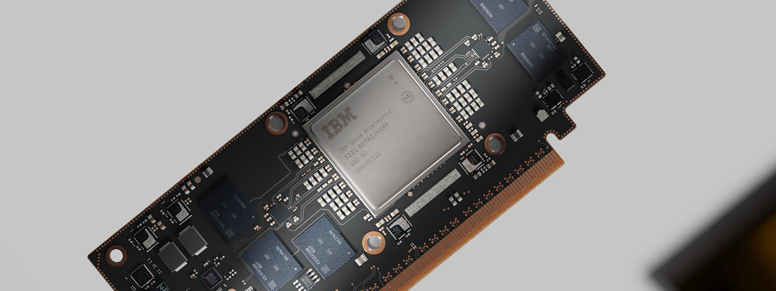
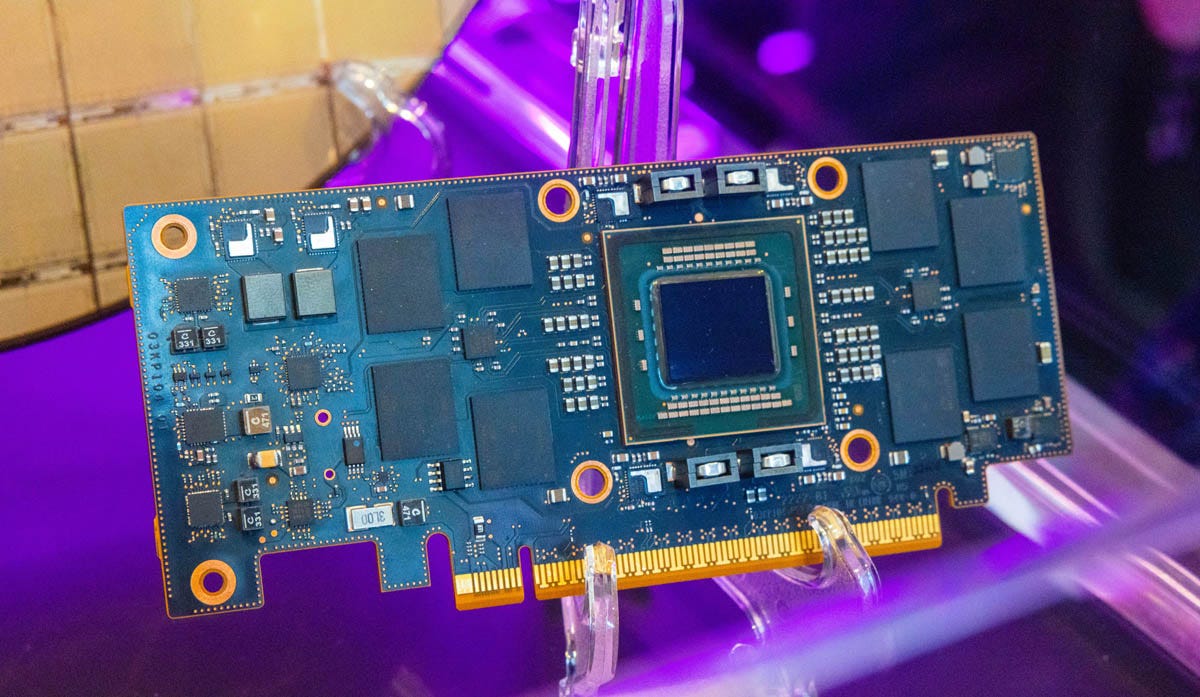
This is not a GPU, and it is not trying to be. Spyre is a 75 W single-slot PCIe inference card, designed to fit in IBM Z and Power systems.
-
Spyre is already shipping in systems. This overview is a summary of a detailed technical disclosure at ISSCC 2026.
-
The 8-year development timeline is real and deliberate. IBM ran five generations of silicon across three process nodes before releasing the production chip.
-
The single most important design constraint is the absence of an auxiliary power connector. Every architectural decision flows from that 75 W PCIe slot limit.
-
The dual-loop power management system is the most interesting technical contribution in the ISSCC 2026 paper. It is not a marketing feature because it delivers measurable throughput gains over the single-loop approach IBM used previously.
IBM presented its Spyre AI SoC solution for inference at ISSCC this year, capping off what the company describes as eight years of silicon development. The concept of Spyre dates back to around 2015, when IBM Research described starting a hallway conversation about low-precision computing. The first early prototype was shown at VLSI 2018, before most of the industry had decided that dedicated inference silicon was worth building.
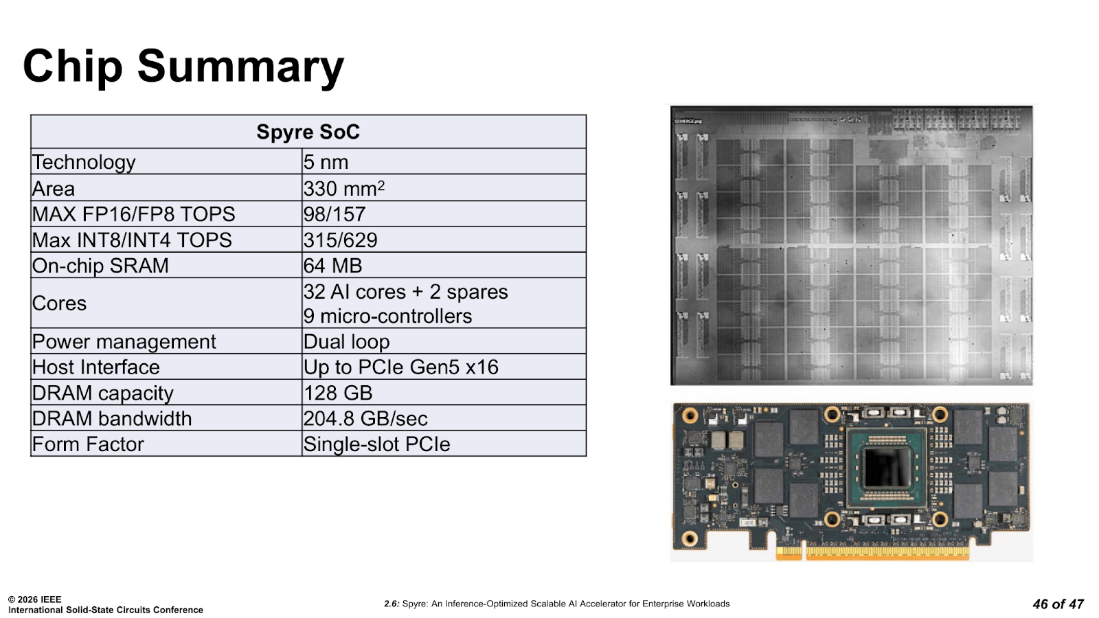
The first production chip, a 330 mm² 5nm SoC with 25.6 billion transistors became commercially available in 2025 for IBM z17 and LinuxONE 5, with Power11 following at the end of the year.
The general story of the march of machine learning started with AlexNET in 2012, and the evolution ever since has been parallel tracks of hardware getting faster and more optimized, or models pivoting from convolutional neural networks to recommendation engines, embedding tables, or transformers. Models such as GPT-2 and BERT had not yet evolved into enterprise staples in 2018, and most people in the industry assumed CPUs would handle a good amount of datacenter inference well enough.
IBM, along with others, started building out its test silicon to offer a more efficient solution. Initially as a test project internally (Intel does a lot of those), Spyre would appear to be the start of a commercial success for IBM as it pairs the hardware with its systems but also for the back-end of its consultancy business.
What IBM Was Actually Building Spyre For
Before getting into the Spyre chip itself, it is worth being precise about who this is actually for, because the use case shapes every decision for a chip like this.
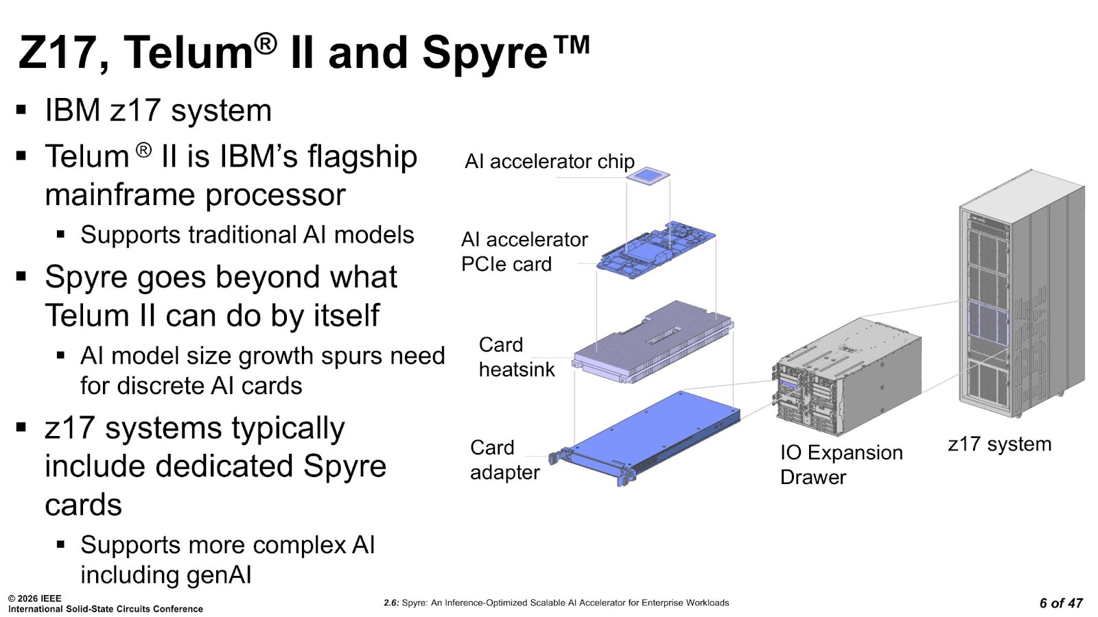
IBM’s mainframe customers include many major banks, insurers, and governments running mission-critical transaction processing at enormous scale. A large bank processing credit card fraud scores needs to evaluate every transaction in milliseconds, at tens of thousands of transactions per second. These heavy encoder-class workloads, primarily BERT variants and similar models, have always been the bread and butter of IBM Z’s AI acceleration, going back to the on-chip accelerator in Telum. The architecture in Telum and Spyre are more than similar, allowing workloads to migrate between the two depending if latency or performance are needed.
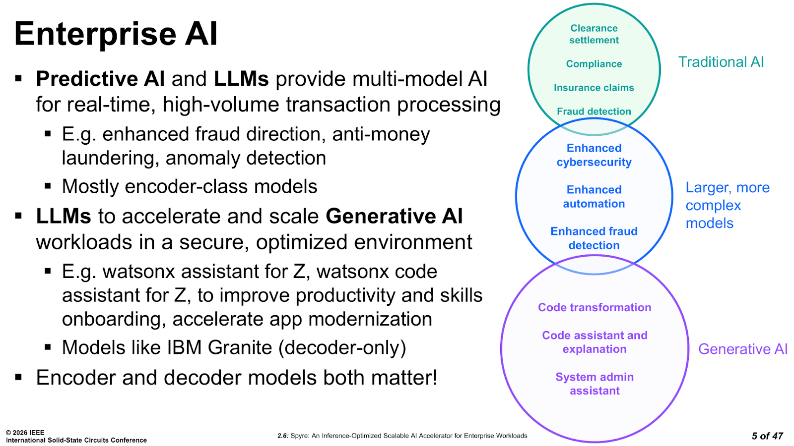
Spyre extends the CPU AI acceleration, adding capacity for larger and more complex models, and proper generative AI support for decoder-class workloads. This means it can keep up with their token-by-token generation and the different memory requirements, which require reliable, precise hardware that can keep up.
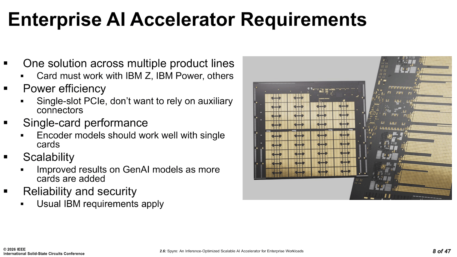
The key constraint baked into Spyre from the start was that the accelerator needed to fit inside its IBM Z and Power systems without the need for dedicated power infrastructure. A single PCIe slot, with no auxiliary connector, and with a hard 75 W ceiling. There are comparisons that could be made to Nvidia’s T4 or L4 class of server GPUs, as you get an idea of the design space, although Spyre ends up fitting in a rather different place within it.
Five Silicon Generations Before Production
IBM’s development approach here with Spyre is not common in the current shape of the AI industry. Most companies go from first architecture to production silicon within about two or three years – startups especially will launch their first generation silicon, for example. But IBM’s presentation claims it spent eight years and ran through five generations of test/research chips before the enterprise department decided to adopt it for their portfolio.
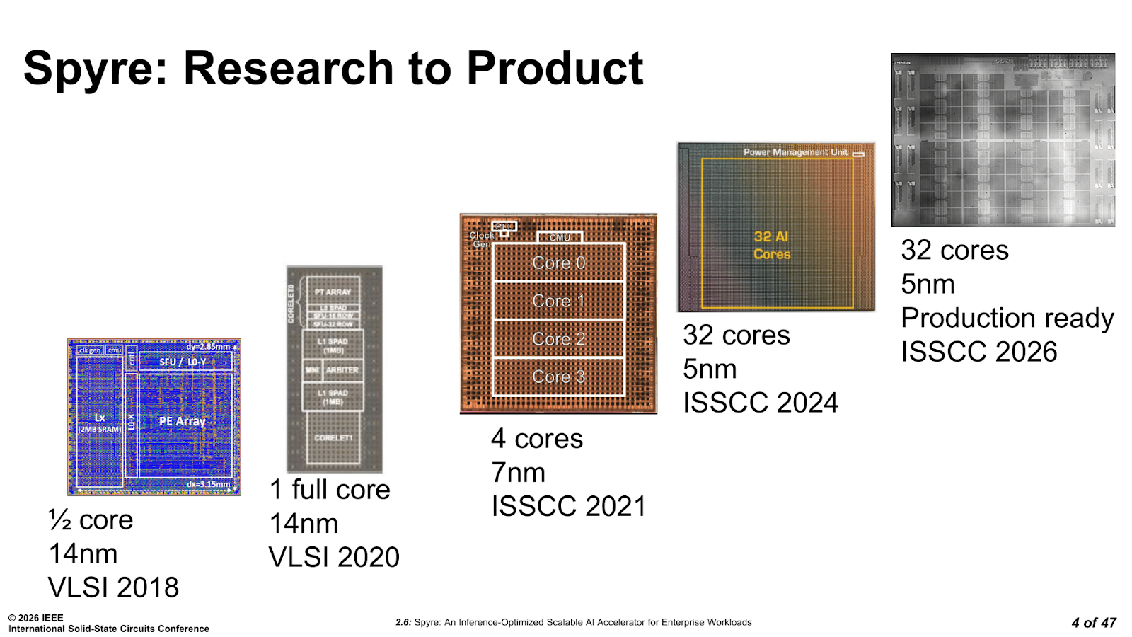
The 14nm half-core demonstrated back during VLSI 2018 proved the concept of a programmable dataflow architecture. A full 14nm core with a two-corelet structure followed in 2020, then we saw a 7nm four-core chip debut at ISSCC 2021, providing IBM with real-world data on crossbar bandwidth and memory latency across multiple cores. A larger 32-core on the more dense 5nm SoC with full power management was shown at Hot Chips 2024, two full years before the production chip launched commercially.
Moving from that 2024 research within its SoC to the production part is a less risky step than jumping straight from architecture to tape-out, and that is precisely the point. With an architecture now capable in tapeout, the enterprise team were able to add the RAS features needed to make it suitable for IBM’s high-performance portfolio.
The Spyre SoC Architecture
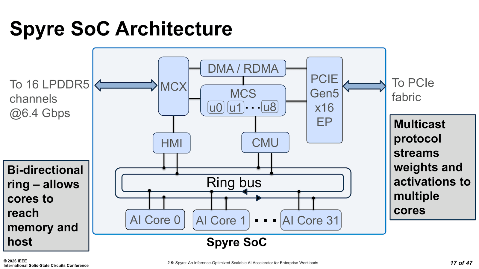
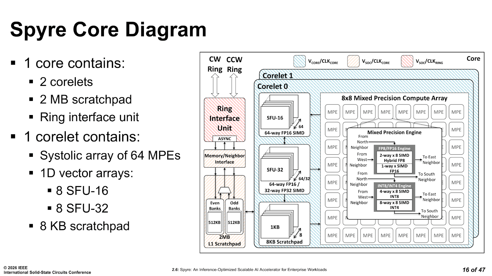
Looking at the finer details within the Spyre SoC’s architecture, it has 32 active AI cores arranged in an 8×4 grid, plus two spare cores dedicated to yield.
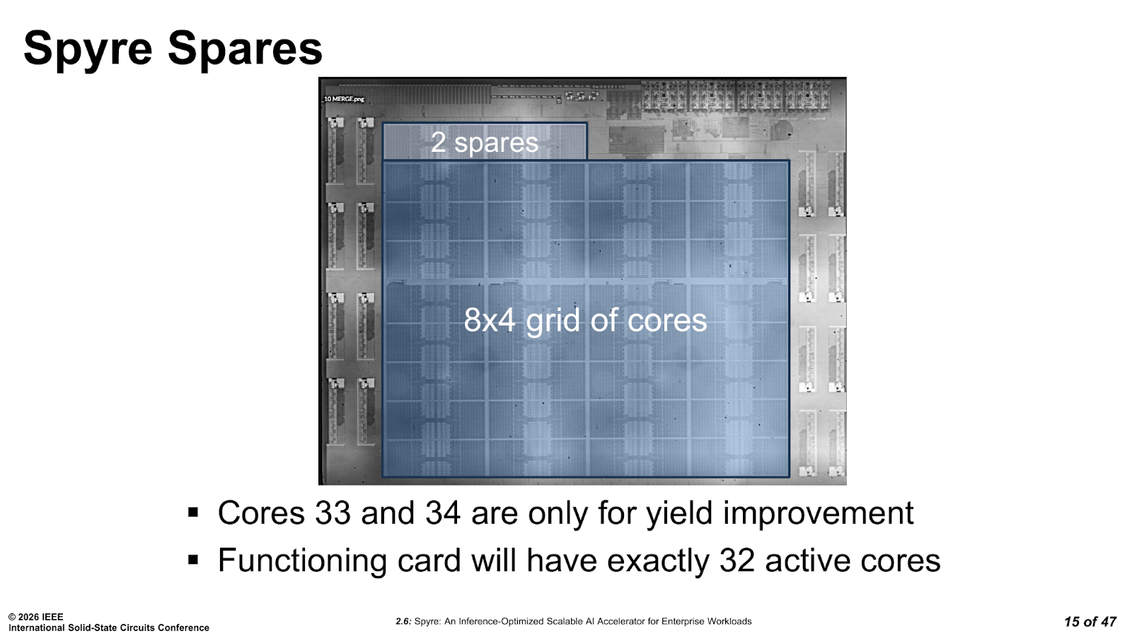
This means theoretically that if one or two cores fail during manufacturing, the chip can still ship as a full 32-core part. All 32 active cores are connected via a bidirectional ring bus, and the full core array carries 64 MB of on-chip SRAM.
Each AI core is split into two corelets, each with 2 MB of L1, and each corelet contains a 2D 8×8 SIMD-systolic array of 64 low-precision math engines that handle the bulk of the matrix multiplication and convolution workloads. Alongside the 2D array, there are 1D vector arrays with FP32 capability that are used for activation and normalisation functions when lower-precision formats are not accurate enough. Supported formats include FP8, FP16, INT8, and INT4, which cover the quantisation options that typically matter for modern inference across both encoder and decoder model types.
According to IBM’s disclosure, the Spyre SoC’s peak throughput sits at
-
98 TOPS at FP16,
-
157 TOPS at FP8,
-
315 TOPS at INT8, and
-
629 TOPS at INT4.
IBM compares the chip to NVIDIA’s 72 W inference card, the L4. Spyre’s peak is 315 TOPs at INT8, for 4.2 TOPS per watt, rather than the L4 which has a peak at 242 TOPs at INT8, for 3.4 TOPS per watt.
IBM’s own data disclosed at ISSCC 2026 takes it one step further, claiming 2 to 3x better power/performance than GPUs using encoder-class models, though those figures are measured on IBM’s specific workloads and aren’t using a cross-benchmarkable metric that can be directly compared.
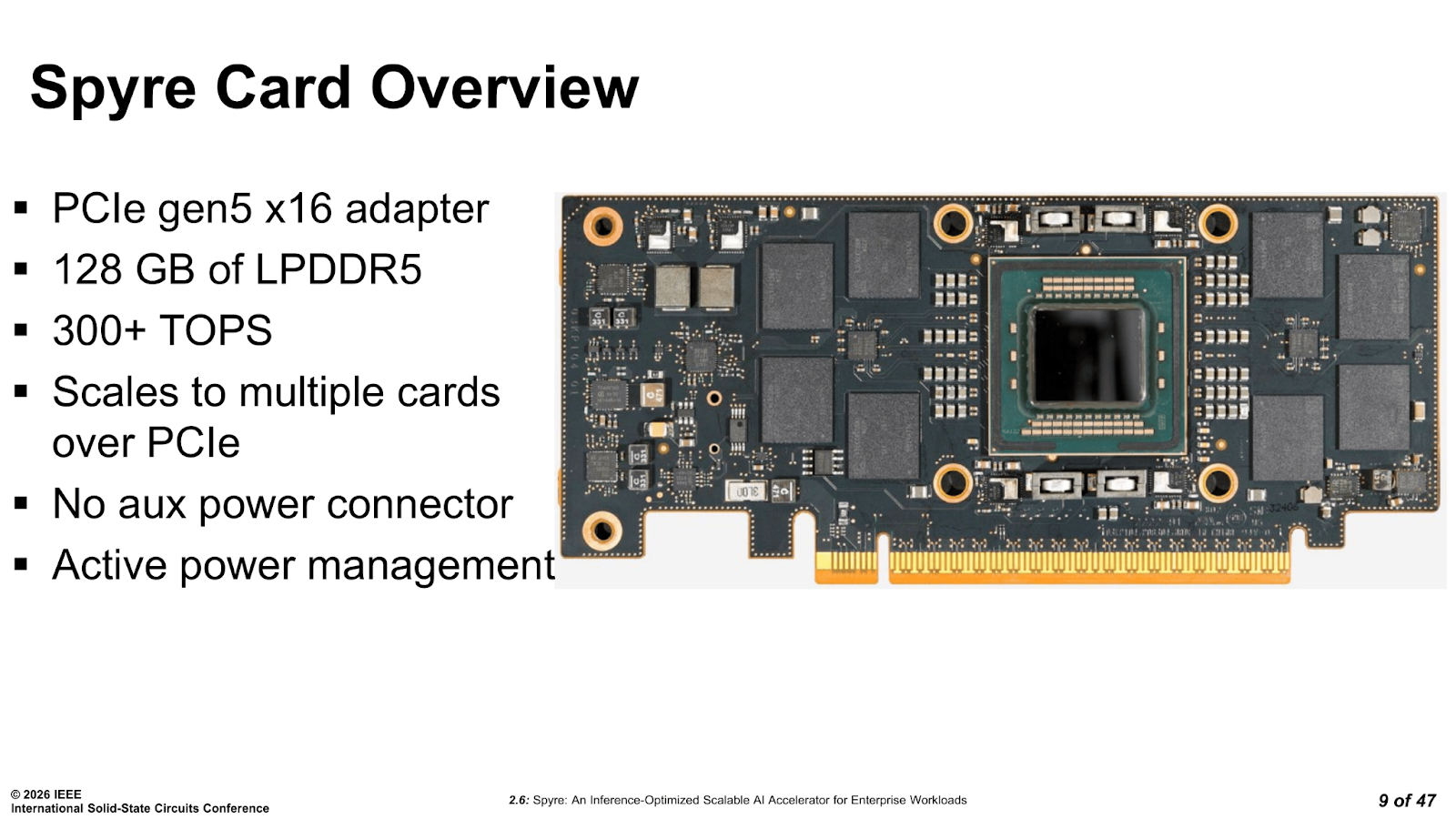
Moving on to the memory subsystem, the design choice is driven entirely by the 75 W power constraint. While HBM offers the level of bandwidth throughput engineers typically want at their disposal, it draws too much power and requires more complex, and expensive packaging that simply does not fit within Spyre’s budget. IBM went with LPDDR5 instead, with 16 channels running at 6.4 Gbps, delivering 204 GB/s of peak bandwidth and 128 GB total capacity per card, with SECDED ECC protection for all of that available DRAM. The 8 dual-channel LPDDR5 modules sit on the PCIe card alongside the SoC itself and aren’t packaged on top of it, or within it.
That 128 GB figure is also an important number in the generative AI discussion. Compared to the NVIDIA L4, which only has 24 GB..
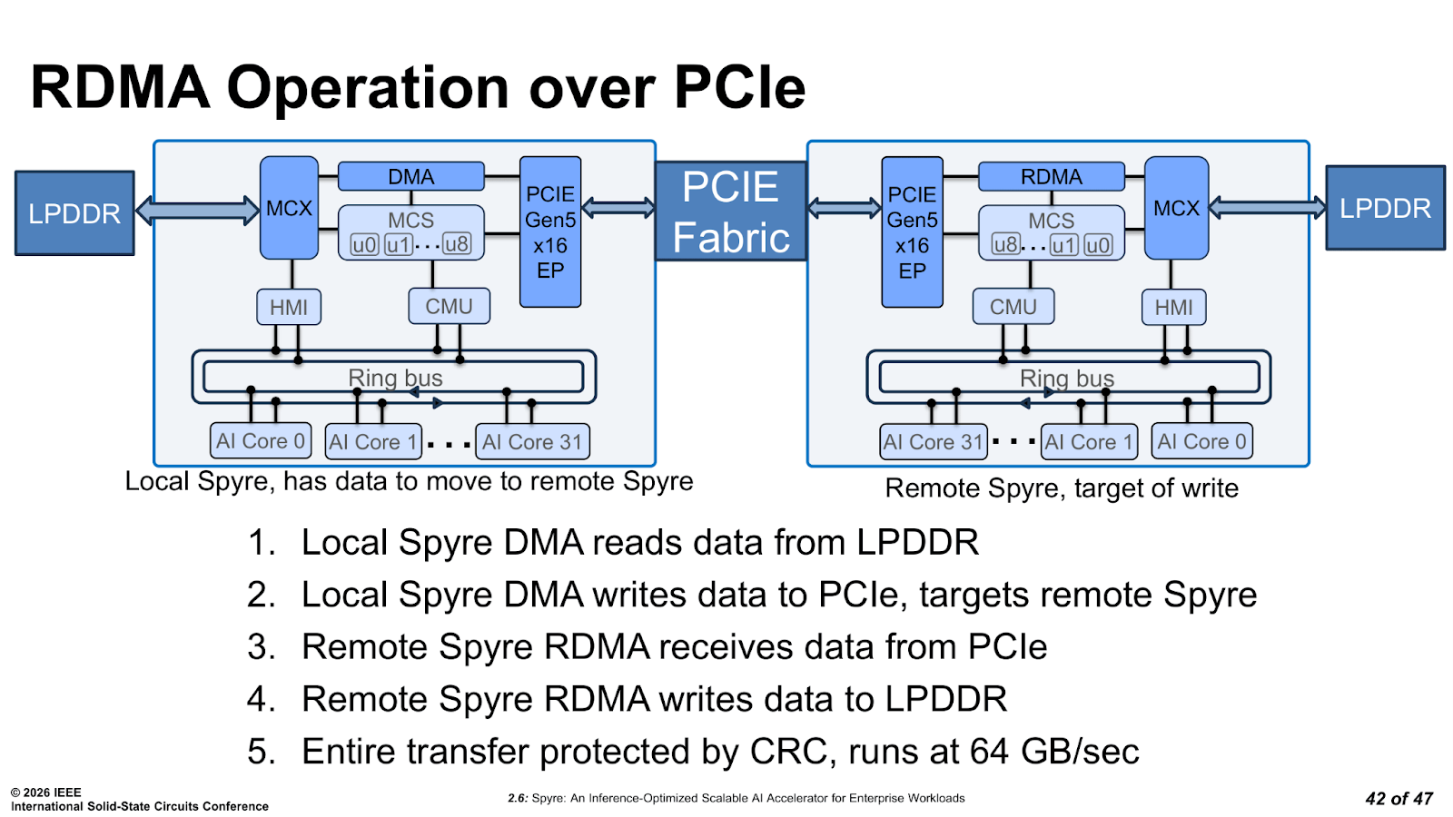
PCIe connectivity is Gen5 x16, giving 64 GB/s of host bandwidth in and out. The RDMA engine is also worth noting, as it allows multiple Spyre cards to transfer data directly between each other over PCIe without any host CPU involvement, which is how multi-card scaling works without turning the interconnect directly into a bottleneck.
How IBM Spyre Deals With Power Management
Spyre’s dual-loop power management system is the most technically interesting part of the overall design. AI inference workloads have a highly variable power profile, and INT8 matrix multiplications can push the power and stress on the circuits.
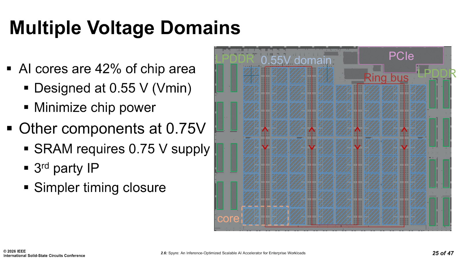
By using compute design enabled for low voltage operation, the idea is to extract efficiency out of the design. 0.55 volts as a voltage minimum on compute IP for a modern process node is really low, almost DSP levels or even bitcoin ASIC levels. Modern high-performance IP often sits around 0.7 volts to 1.1 volts and the power scales with it. Designing low Vmin circuits is a skill in-of itself, but the tradeoff is often lower peak frequencies. The design here was to ensure fitting into that 75 watt power envelope anyway.
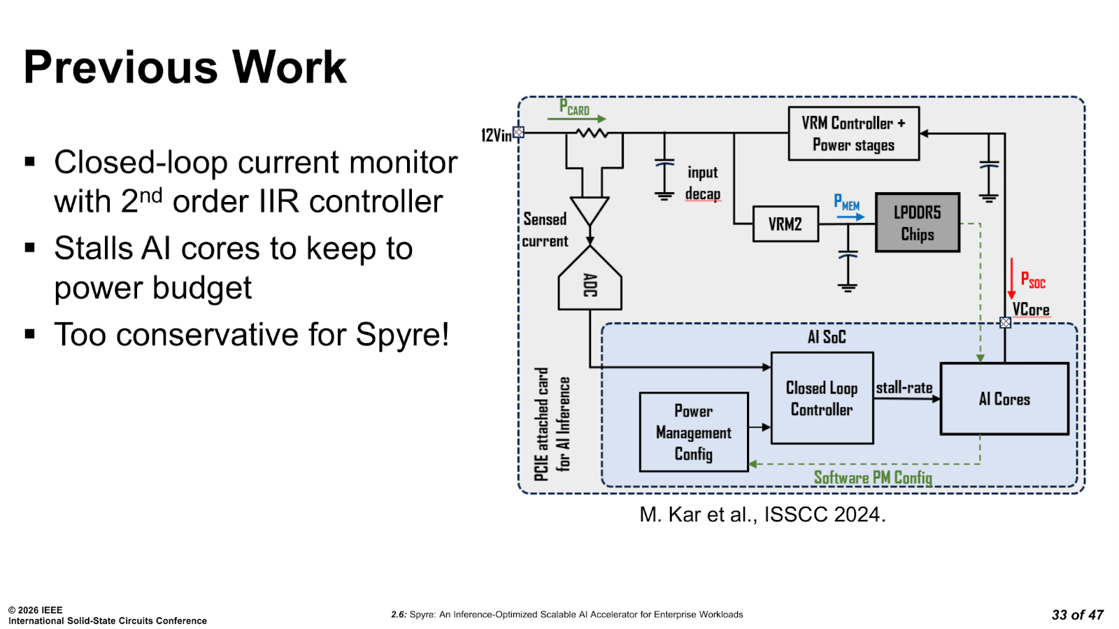
IBM’s previous approach required using a single closed-loop IIR controller that stalled AI cores when the power budget was nearly exhausted, similar to a time-muxing or duty cycle. This method works, but it is conservative by design, and means that throttling is based on a single set point at a single time constant.
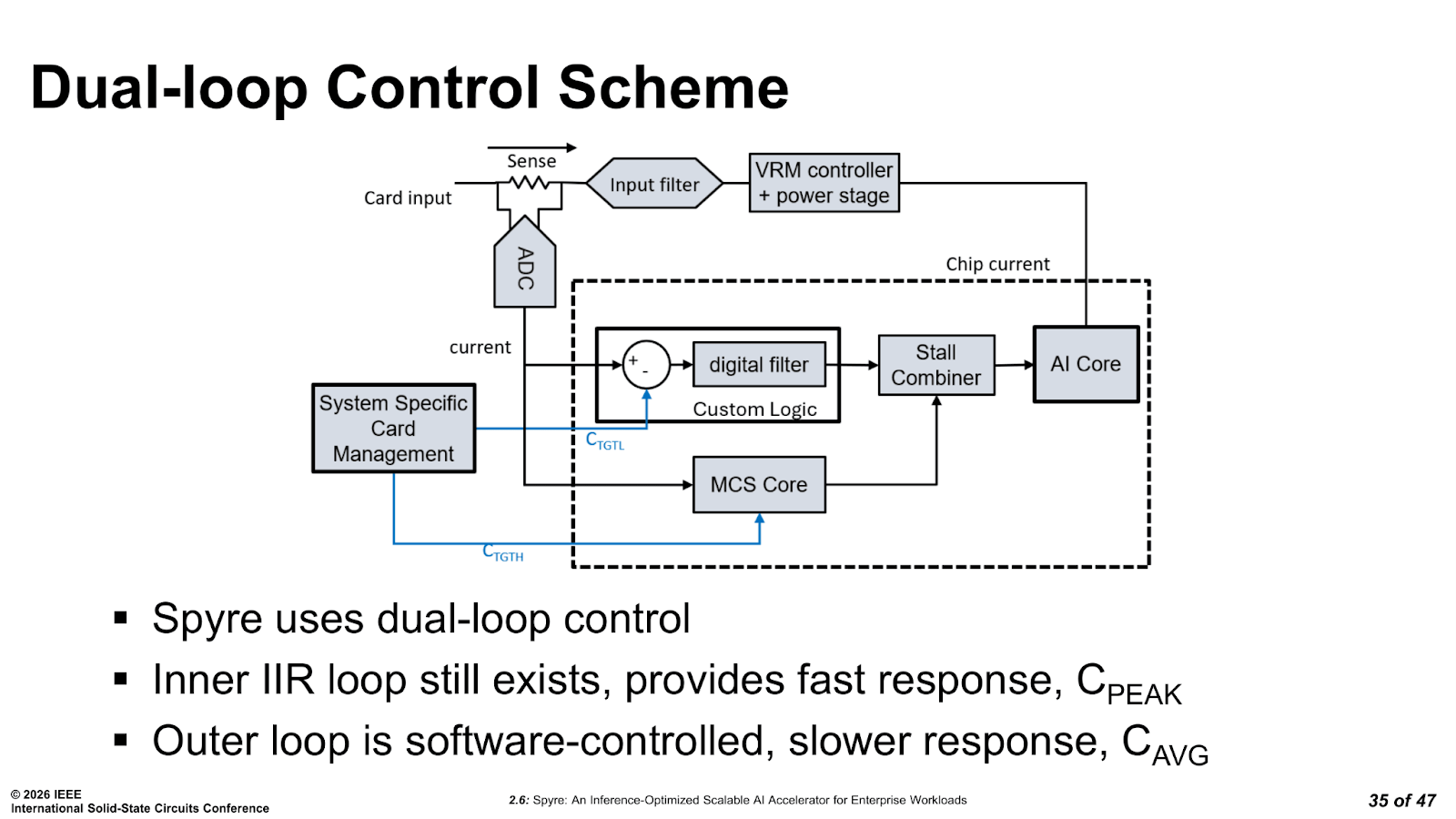
Spyre replaces that completely with a dual-loop system: a fast inner loop handles peak-current spikes on short timescales, and a slower, software-controlled outer loop adjusts the average-current target based on actual workload behaviour in real time. The two loops operate with different time constants and setpoints, allowing the system to use the available power headroom safely during short bursts without violating average power limits over longer power windows.
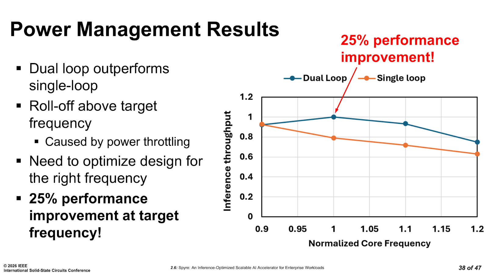
The result, based on IBM’s ISSCC 2026 data, is a 25% higher inference throughput compared with using a single-loop controller under the same power budget. For encoder models, the boost ranges from 7 to 32% depending on sequence length and configuration. That isn’t just a trivial gain for the sake of it, and it also requires no changes to the silicon whatsoever.
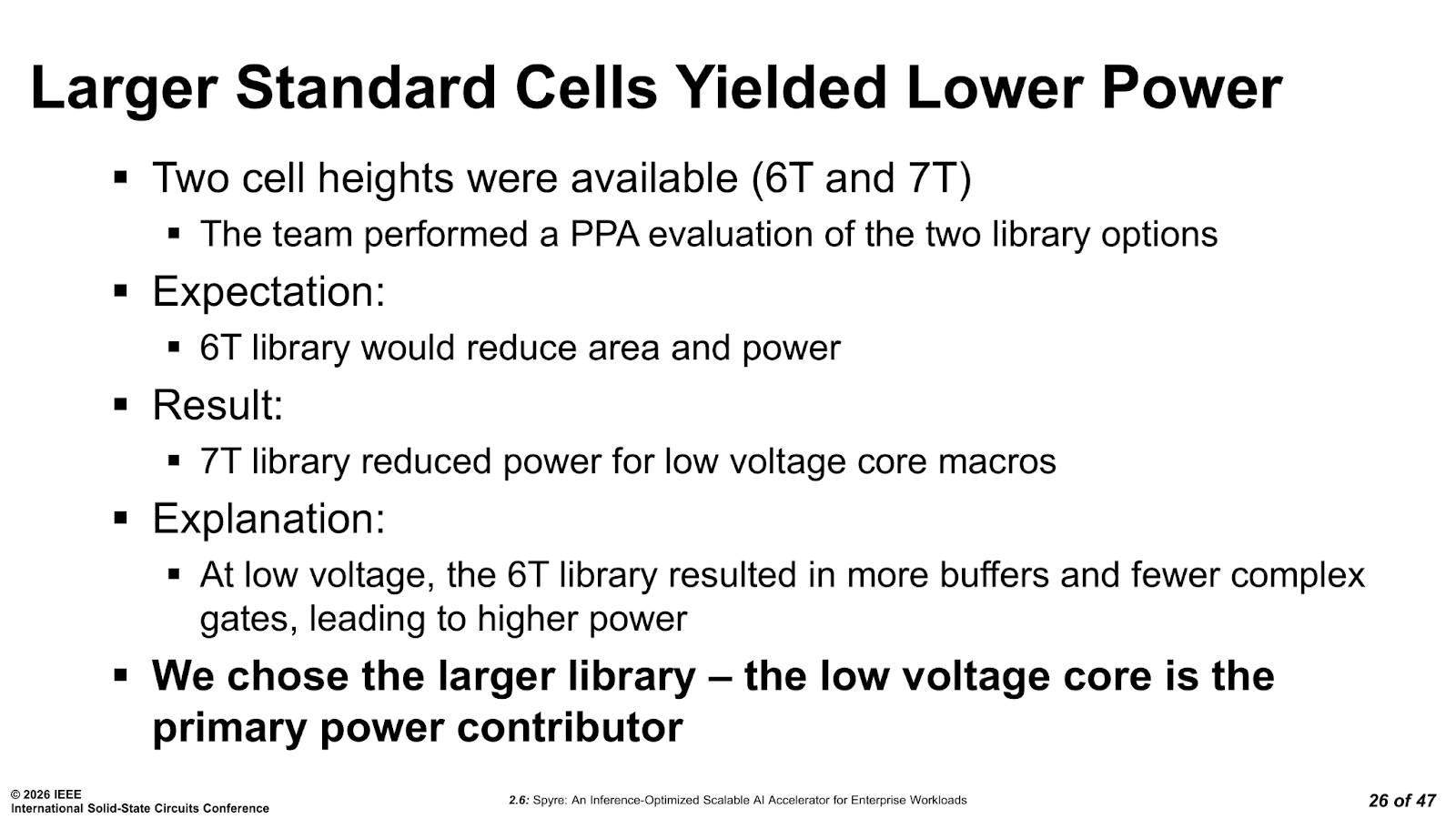
Before taping out, IBM also made several design decisions to reduce the overall baseline power. The AI core array itself runs at 0.55V while the SRAM and third-party IP blocks run at 0.75V. IBM also made the counterintuitive choice of the larger 7T standard cell library over the denser 6T option, because testing showed that the 6T library actually drew more power at 0.55V due to the need for additional buffers. A total reduction of 9% in synthesis frequency target before tape-out managed to cut power by 7.5%, with re-synthesis adding further power and area savings of around 8% and 6% respectively.
Scaling Beyond One Card
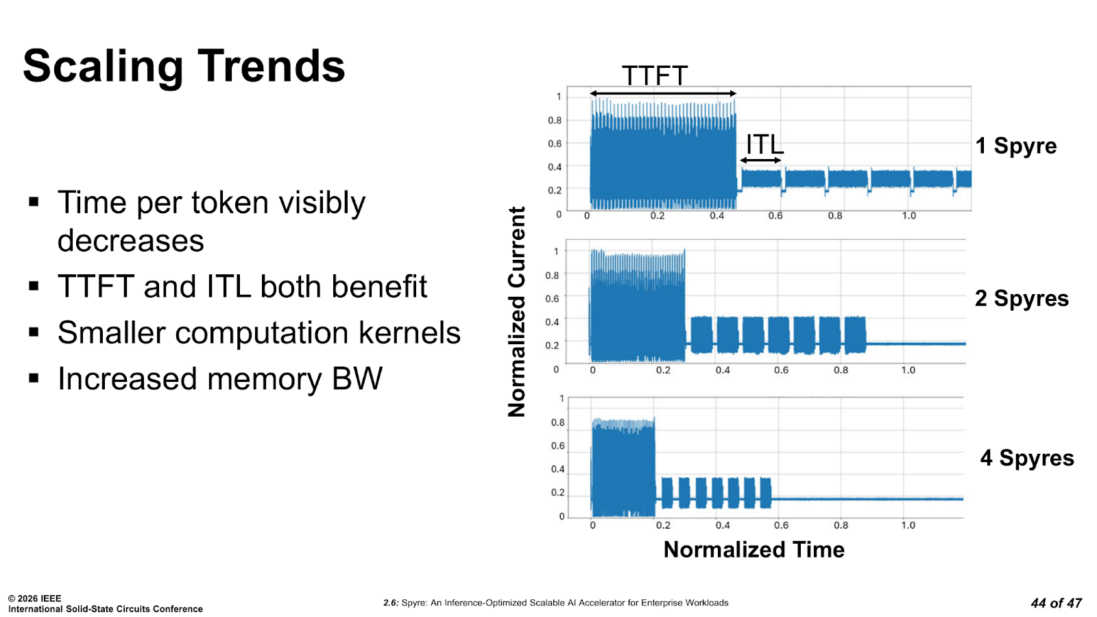
A single Spyre card handles encoder workloads comfortably within its memory budget, and while typically large generative AI models are a different proposition altogether, many simply do not fit in 128 GB before batching is even considered. IBM addresses this through RDMA-based multi-card scaling, in which multiple cards communicate via a PCIe switch, enabling direct card-to-card RDMA transfers at 64 GB/s with CRC protection, bypassing the host CPU entirely.
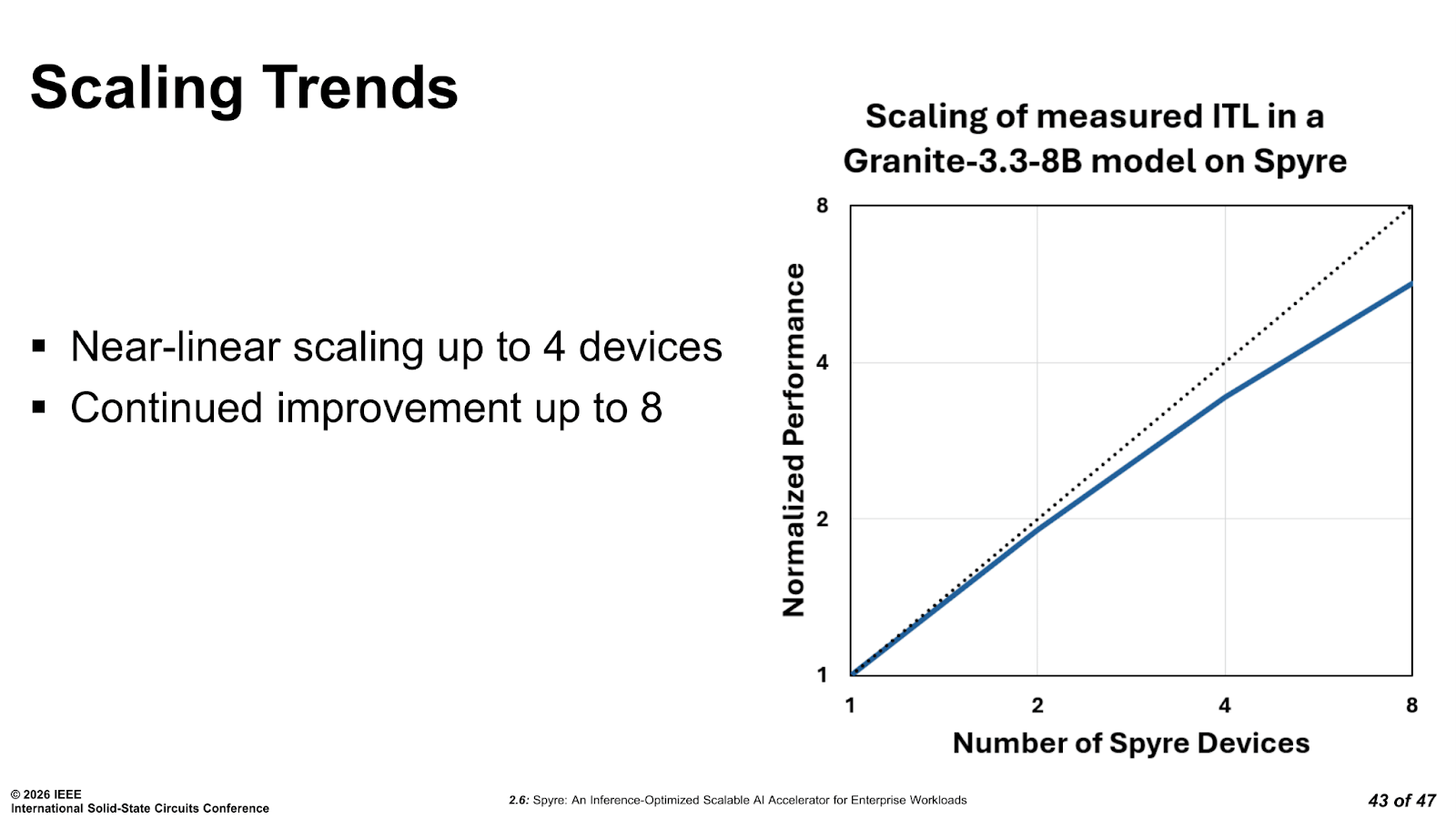
IBM’s published data for its optimized Granite-3.3-8B model show near-linear scaling with four Spyre cards, with continued gains extending to eight. As cards are added, each one handles a smaller compute chunk, the total memory bandwidth aggregates, and both time to first token and inter-token latency improve in parallel.
A fully loaded IBM z17 supports up to 48 Spyre cards per tray, 192 cards per system. That puts 6.1 TB of accelerator memory inside the mainframe’s security boundary. IBM Power11 supports up to 16 cards per system. No comparable GPU server configuration delivers 6 TB of accelerator memory within a single system at enterprise-grade reliability and security.
What Spyre Is and What It Is Not
While NVIDIA’s high-end hardware runs anywhere from 700 W up to 1200 W in the most dense systems. In the future, that is set to scale up multiple kilowatts per chip. Comparing Spyre to an H100 for example on TOPS isn’t really any kind of comparison that anyone should be making. They are built for completely different environments with completely different constraints.
The relevant comparison is in single-slot enterprise inference cards, where power efficiency and memory capacity per watt matter more than raw throughput. In that space, 128 GB of LPDDR5 at 204 GB/s within a 75 W budget is a strong position. NVIDIA has its options, but IBM also sits in a busy market with a number of inference focused cards from 75 W up to 300 W from startups such as Tensordyne, Tenstorrent, d-Matrix, Rebellions, Furiosa, Qualcomm, Taalas, Positron AI, etc.
One of the key aspects today is the disaggregation of transformer workloads between prefill (compute bound) and decode (memory bandwidth bound). IBM doesn’t particularly isolate Spyre into one of those buckets, showcasing that for its workload portfolio, it can be a one-card solution. As workload disaggregation understanding improves, we might expect to see this to change in the future.
What We Do Know About the IBM Spyre Ecosystem
When then chip was still in the transition from research chip into enterprise product, IBM held presentations about the future of the product line, some of which would be leveraging IBM’s expertise in manufacturing, manufacturing, and system scale.
This is IBM’s Mukesh Khare in 2022, who we’ve interviewed a number of times, showcasing the AIU before it became Spyre. The next year, he discussed that future generations would look to leverage higher speed memory types, as well as packaging chiplets together into one SIP. It’s unclear if the goal is still a PCIe card or if it will move to an OAM form factor that high-powered AI chips currently use. Recently IBM announced a partnership enabling Arm-processing modes to its CPUs, and we have to assume that access to Spyre might become part of that as well.
IBM Spyre SoC: Concluding Thoughts
The primary story for Spyre is very solid, with 8 years of development, 5 generations of test chips, 3 process nodes, and a production design backed by years of real-world hardware data before it shipped out to customers commercially. The dual-loop power management system is a genuine engineering contribution, and the memory capacity advantage over competing single-slot options is a real and meaningful design choice for the workloads it is targeting. Enabling cross-platform deployment across its IBM Z and Power is a sensible strategy through using PCIe looks to have been executed pretty cleanly. PCIe should also mean these cards could work under x86 and Arm, although IBM hasn’t disclosed this use case yet.
What cannot be evaluated yet about Spyre however is whether or not enterprises running IBM Z and Power platforms will adopt the levels of generative AI at the scale where Spyre’s specific advantages become the deciding factor in this form factor. IBM often keeps the consulting business hardware costs close to its chest, so we might never find out!
Update from Ian:
We actually spoke with IBM back in 2024 about its Spyre card, back then called the AIU. You can see all this content on YouTube: