
When people talk about the semiconductor industry, most of the attention goes to the visible parts: the chips, the process nodes, the packaging technologies, the benchmark slides, and the race for more performance per watt. Far less attention lands on the software and infrastructure that makes those chips possible in the first place. But as chip design has become more complex and we drive to more advanced process nodes, the design becomes tightly coupled to manufacturing. Designing a modern processor is no longer just about logic design and timing closure – we talk about advanced packaging, chiplets, multiphysics, IP integration, software driven optimization, and increasingly, the challenge of exploring a design space so large that human engineers alone cannot reasonably cover it.
That is why Synopsys matters. For years, it has sat near the center of modern chip design, providing not just EDA tools but also the IP, signoff, and increasingly the physics aware co-design infrastructure needed to bring advanced silicon to market. A few years ago, I interviewed former Synopsys CEO Aart de Geus about where EDA was going and how the industry was changing.
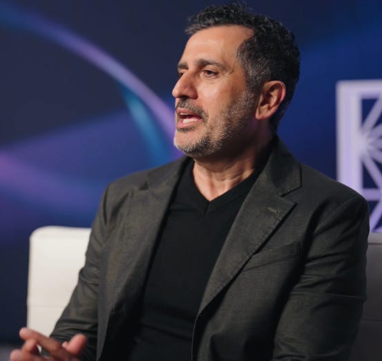
Coming back now to speak with new CEO Sassine Ghazi, the conversation feels both familiar and very different. Familiar, because the core challenge remains helping customers build ever more ambitious silicon. Different, because the problem has expanded. The old model of simply riding Moore’s Law forward is no longer enough. Today, customers are dealing with one year design rhythms, disaggregated architectures, 3D stacking, thermal constraints, and the need to bring manufacturing physics much earlier into the design flow.
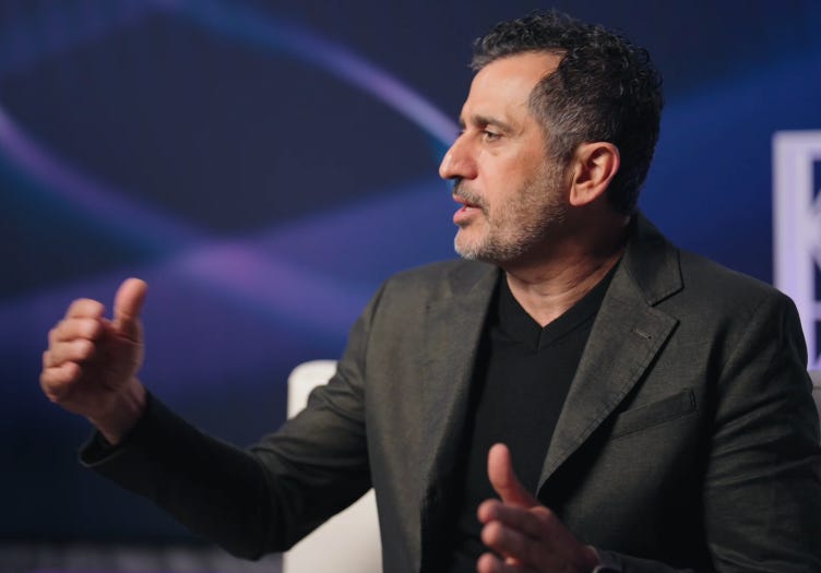
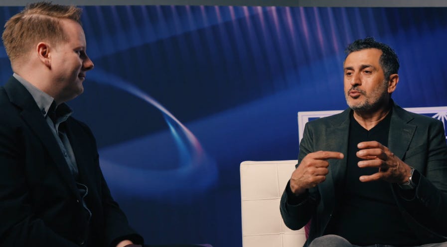
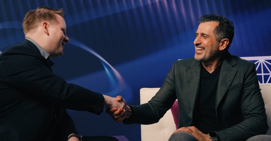
I caught up with Sassine Ghazi just after he came off stage at Synopsys Converge, the company’s annual event, where much of that future was on display. In this interview, we talk about how Synopsys sees the chiplet era, why Sassine says the company did not just embrace that shift but helped enable it, what the Ansys acquisition was really about, and how the industry is moving from simply designing chips to co designing chips, packages, thermals, materials, and software behavior all at once. We also discuss Synopsys’ work with Rapidus as it tries to stand up a new leading edge foundry, and where agentic AI may actually fit into the chip design workflow, beyond the marketing language and into something that can deliver real engineering value.
The following is a transcription of the above video. It has been edited for clarity.
Ian Cutress: Given the nature of chip design, it’s accelerating; we’re all seeing it. Companies are now not only producing more products but also in greater volume. How is the Synopsys business model changing?
Sassine Ghazi: The complexity and pace, that exponential, is getting steeper and steeper.
If we go back 15 to 20 years ago, we followed Moore’s Law – our customers owned their architecture, we provided the software to enable and implement the chip, and then the customer themselves, with the foundry partner of their choice, would manufacture it.
About 10 years ago, the complexity between design and manufacturing became more intertwined. We played a role in optimizing between design and technology. You look at the chips today with the requirements of AI, and the architecture flavors are rapidly evolving. The complexity of getting the power and performance needed is no longer following Moore’s Law, so there are different approaches, advanced packaging, multi-die, etc. You need a very sophisticated EDA and a tremendous number of IPs to connect these chips together. We’re in a unique position because we lead in EDA technology and have the broadest IP portfolio, and our customers have been spending a higher percentage of their R&D on that automation.
Ian Cutress: So time to market is becoming more critical for your customers?
Sassine Ghazi: Absolutely, because it used to be 18 to 24 months to design a chip. Now, customers are working to a one-year rhythm to deliver new silicon, which just means more pressure on everything they do, be it the software we’re providing, or new techniques, to shrink design time.
Ian Cutress: One of the first companies to integrate chiplets through heterogeneous integration had a difficult time doing so because there were very few tools available. These are the sort of tools your company produces. How have you embraced the chiplet era?
Sassine Ghazi: We didn’t just embrace it, we enabled it. Because if you think back to architecture, as you disaggregate from a monolithic to a chiplet, you don’t do this manually. Which part of the chip goes on which technology node? Where do you put it in the stack if you’re stacking in 3D? What is the memory role in it?
We have a technology we call the 3DIC Compiler, where you start from a specification and go architect the advanced package or chiplet, whatever you want to call it, and do the what-if analysis. If I use 5nm for this instead of 3nm, what do I get in terms of power, etc.? Then the connectivity between these chips is a whole new level of complexity; that’s where UCIe was born, with PCIe, HBM, etc., to connect the system together. And it’s a fantastic opportunity, because what we’re seeing now is not only semiconductor companies designing these chips, but hyperscalers themselves moving from general-purpose to ASICs to COT (Customer Owned Tooling).
Ian Cutress: With tools like the 3DIC Compiler – is that something borne out of customer requirements, or did you already have an ongoing internal project to deliver it?
Sassine Ghazi: We see things very early with the customers, and the 3DIC Compiler is a great example. Around 2017, we could see customers looking for different architectures and packaging to achieve better performance and power, rather than relying solely on Moore’s Law. We started exploring and developing the technology back then, before the first adoption came around three to four years later. As that first adoption came in, we discovered a new challenge: physics. Customers exploring manufacturing before going into production found thermal issues, warpage, and die cracking during packaging. Physics needed to be integrated, and that’s where we embarked on truly transforming our company with the acquisition of Ansys.
Ian Cutress: On that front, especially with thermals, I found a bunch of IBM patents on intra-chip cooling from the 90s and 2000s. As we look at multi-stacked chips, the next stage is surely intra-chip cooling, which means you’ll have to model it for your customers.
Sassine Ghazi: Yes, exactly. And beyond modeling, there are certain hot spots on the chip that you don’t want to overdesign for. Do you have visibility into the software that will run on that chip?
So you can design just right, not overdesigning, keeping costs down, but at the same time making sure it’s not heating up when you run a certain corner case.
Ian Cutress: That means if you’ve got a workload that attacks the ALUs or the memory in a certain way, can you design for that workload, but then you might end up with a workload-specific chip?
Sassine Ghazi: Exactly, otherwise, you just overdesign, and when that happens, not only is it expensive and time consuming but the chip is not competitive either because you’re building so much margin between its different functions. What we announced today, our Multiphysics Fusion platform, is about bringing those physics models into the design phase itself, taking into account the IR, the thermal, the electromagnetic, and the mechanical, so you’re co-designing rather than overdesigning. We introduced that concept with the fusion platform. Ten years ago, the challenge was less about physics and more about how do I close the timing on the chip, how do I close the power?
Ian Cutress: Does wafer scale present any additional problems?
Sassine Ghazi: The challenge is more how do we model on the manufacturing side at the device physics level, and then at the packaging level. At the architecture level, if you’re designing it with that architecture, is this the best representation of the physics that you’re going to manufacture with? So in a sense, yes, but from a Synopsys point of view, we look at it as DTCO (Design Technology Co-Optimization). With the various flavors and models of the physics and what our foundry partner is going to be providing as a solution.
Ian Cutress: In terms of EDA and especially IP, getting it to work on a specific process node is a key aspect of the product. But a lot of what you’ve spoken about today, and a lot of what we’ve discussed, is almost process node agnostic. So how much do the foundry players get involved?
Sassine Ghazi: That’s true for IP, in a sense. We have the broadest IP portfolio, but we have to provide it to our customers on the various technology nodes with various foundries, otherwise you’re not the leader in IP. If you say I’m only doing it for that one node with one foundry, then customers will end up building their own IP. So the work we do with multiple foundries requires a lot of close partnership and collaboration, because we’re there at a very early stage of their PDK development, etc. Same on the EDA tool side, when we are designing Fusion Compiler, or for that matter, PrimeTime or RedHawk, etc, you need to know what implementation of materials and physics they’re using, so you’re designing the tool and the algorithm to match it.
Ian Cutress: So we’re even talking about what material they’re using for liners and interconnects within the chip. Because that’s all the physics of how these metals work.
Sassine Ghazi: Our tool implements it because the customer has a requirement. They design it at, and I don’t want to oversimplify what the customer is doing, but you kind of said it. The software we provide, it could be argued, is as complex as what our customers are trying to do. But we are the bridge between that architecture and if you can manufacture it, that’s where the signoff strength comes in.
Ian Cutress: On foundry, Rapidus is the first new leading-edge foundry from a new entrant into the industry, I would argue perhaps the last time that will happen in my lifetime! From your perspective, does working with a new partner on leading-edge IP introduce challenges compared to someone who’s been doing it for 20 years? Can you go into how you’re working with them?
Sassine Ghazi: We have a fantastic relationship with Rapidus. When I talked to our Japanese team, I said Rapidus is a gift for us, especially when it comes to Japan as a starting point. Of course, they’re not going to be a foundry just for Japan; they have an ambition to be a global foundry. The reason I say it’s a gift, from a technology point of view, they have a partnership with IBM on process technology. We have a technology called TCAD (Technology Computer-Aided Design), which models the device and the process technology when the technology is at the R&D level. So before you go anywhere near production volume. We started that engagement at that level. Then, as the technology matures, when you’re doing a test chip, the design representation is a PDK (Process Development Kit), and you start from a 0.1 PDK, then evolve to 0.5, 0.7, etc. So we’ve been working very closely with them on both the technology process level, through EDA and design, and to IP.
Ian Cutress: But does it change because they’re new into the industry? Because what you’ve just described is what you do with every foundry when they have a new node.
Sassine Ghazi: Sure. Other foundries go from node to node to node – there is that incremental and cumulative learning. Here, some of that cumulative learning came from their partnership with IBM. But of course, it takes longer because that is the first node they’re creating. The nodes that follow from Rapidus will be exactly like other foundries. From a Synopsys investment point of view, it’s a higher investment, but that’s where we bring tremendous value to that foundry: our tools have seen everything from planar to FinFET to Gate-All-Around, so we’re not reinventing anything in our product.
Ian Cutress: If I look back to 10 years ago, and we had a discussion then about the next 20 years of EDA, we would have arguably said we expect more of the same with incremental increases. But now we’ve got new degrees of freedom in multiphysics and 3DIC and verification and simulation. The question then becomes, what are the next five years going to look like?
Sassine Ghazi: The reason we shared the framework for agentic AI last year is that there is no question that we see it as a significant opportunity. We introduced reinforcement learning into our product in 2020, with general market availability, and we started investing in it around 2017. Looking back over the last three years, the speed at which models are innovating, the way the orchestration of models is evolving, and the opportunities it’s providing are unbelievable. A big part of our roadmap is looking at the entire chip workflow and asking which parts of it can be assigned to an agent. We call them agent engineers. How much can you have an agent managing an agent, i.e., orchestrating these agents. What we announced earlier today is the first level of multi-agent adaptive dynamic orchestration. These agents are learning as they operate on new data and new requirements, and on how to achieve the final goal and target. The innovation will continue at a very fast pace. The key, which is the layer that we’ve invested in, is to move every part of Synopsys, every product, every solver, to be working with the latest AI technology, like reinforcement learning or other technology that is available.
Ian Cutress: So you’re talking about an agent calling a solver, getting a result, examining the result, and then maybe calling the solver again, iterating and learning?
Sassine Ghazi: Exactly. What we have today are these task agents, or agent engineers, where the human engineer assigns them a task, they go off and come back with an outcome, and then the human engineer makes changes, etc. There’s a cognitive layer, and the orchestration layer can be adaptive; that’s where we have partnerships with Microsoft, NVIDIA, and others. They’re doing a very good job racing ahead with that cognition and orchestration layer. So we’re not trying to reinvent what is already out there, but rather what do we need to do with our core assets, which is the solver, and bring in AI to accelerate.
Ian Cutress: You have to promise me something, because if I were being facetious, I would say that sounds like a middle management pyramid scheme of orchestration. So, as best as you can, please don’t make it that!
Sassine Ghazi: Oh, you’re talking about the agent of agents as the orchestrator?
Ian Cutress: Yeah.
Sassine Ghazi: The knowledge actually doesn’t decrease as you go up the agentic workflow; it’s the opposite. The reason I was very specific in the words we used earlier today, it’s a dynamic adaptive orchestration. That sophistication in technology to optimize. I was talking to a customer before my keynote, and one customer who’s testing these things said it’s impossible for a human to look across that huge space. So that’s not an agent engineer competing with a human, it’s exploring a much larger space and seeing what is possible. So yeah, definitely it’s not a management scheme.
If you want to catch what’s happening at Synopsys Converge, please check out the links below.