
Five Things You Should Know Before Reading:
-
“3D HBM” Now Feasible: Offers improved AI performance and utilization.
-
But Temperature Is A Problem: HBM-on-Logic exceeds safe temperatures.
-
Thermal Mitigations Are Essential: imec outlines five-ish steps to solve the issue.
-
Lower Clocks: Halving the frequency provides the largest thermal relief.
-
Questions on Cost and Yield: …it might not be worth it, commercially.
Today’s guest post is from Gavin Bonshor, former Senior Editor at AnandTech. Gavin has almost two decades of experience in competitive analysis of high impact consumer and enterprise semiconductor products. Gavin has represented the UK in competitive overclocking, and the art of extracting performance through frequency and extreme sub-zero cooling, holding a number of national records.
If there’s one thing that every tech conference presentation highlights, it’s the fact that AI workloads are constantly scaling beyond current hardware capabilities. Specifically, AI accelerators in this space are hitting physical limits in all areas at once, including power density, memory bandwidth, and complexity. As the long-established 2.5D co-packaged HBM model is still ruling the roost but by some is limiting, the concept of combining accelerator and HBM in 3D is starting to gain traction. With more advanced memory stacking technologies, the challenges faced by the industry to increase memory bandwidth while remaining efficient are becoming ever more prevalent as we advance through the need for more high-performance and efficient compute.
On the road to a HBM-on-logic era, imec turned up to IEDM 2025 with a paper showcasing some really interesting work. It had a bold claim in the title: “Breaking Thermal Bottleneck in 3D HBM-on-GPU Integration”. Big claims require big evidence, and this was a title that immediately caught our eye.
imec presented a paper at the conference to say that it had mapped out a viable thermal path to fully stacking HBM directly on top of an accelerator, and with it answering one of the biggest questions in high-performance at present: can the industry actually move to a true 3D GPU packaging without effectively cooking the silicon on the world’s most expensive BBQ? imec’s answer is essentially yes, but only with major changes. These include adjusting the layout substantially, which might require more than just a simple LEGO brick approach.
Step One: Set Some Ground Rules
Before diving into imec’s vast array of mitigation strategies for validating a proper true 3D HBM-on-GPU stack, it’s important to understand the baseline they are using. The study uses a sophisticated theoretical multiphysics model to create a detailed thermal heat flow template what the 3D GPU might look like. This means a singular high-powered compute die consuming ~400W, with multiple 12-Hi HBM stacks. The simulations compare different configurations use four traditional memory modules (more on that later), along with a conventional liquid-cooled cold plate designed to dissipate heat.
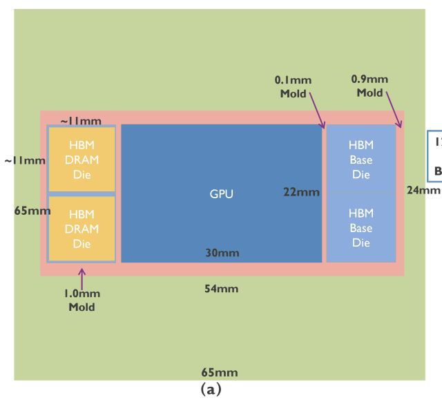
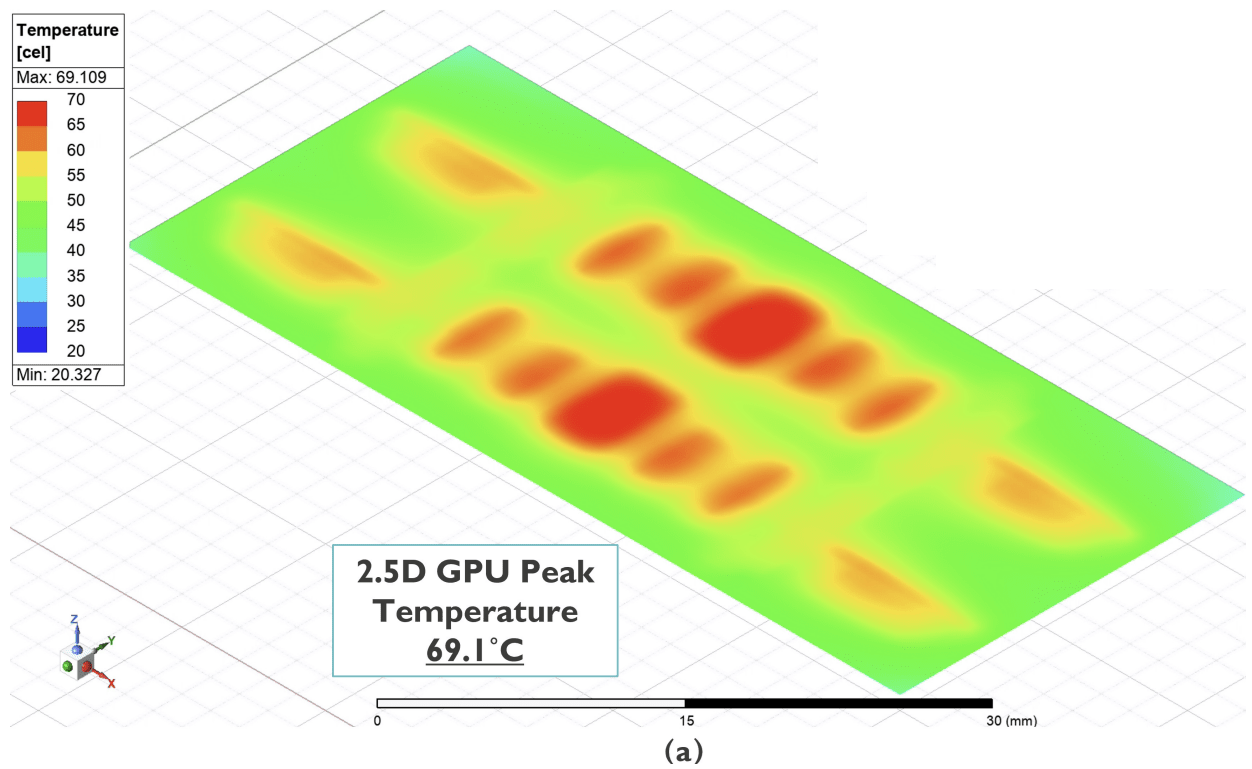
The baseline puts these four stacks in a traditional 2.5D configuration, with a HBM4-like base die underneath each HBM stack. In this configuration, their simulation shows a peak GPU temperature of 69.1ºC, with the HBM silicon reaching around 60ºC in its worst case.
imec’s cooling solution for this (and the other data in the paper) are intentionally designed to be generous, given the level of heat generated from this type of design. On top sits a liquid-cooled plate, rated at 30 W/cm² per Kelvin difference between the coolant and cold plate. This reflects a best-case cooling scenario that might be deployed within today’s high-end AI inferencing juggernaut systems.
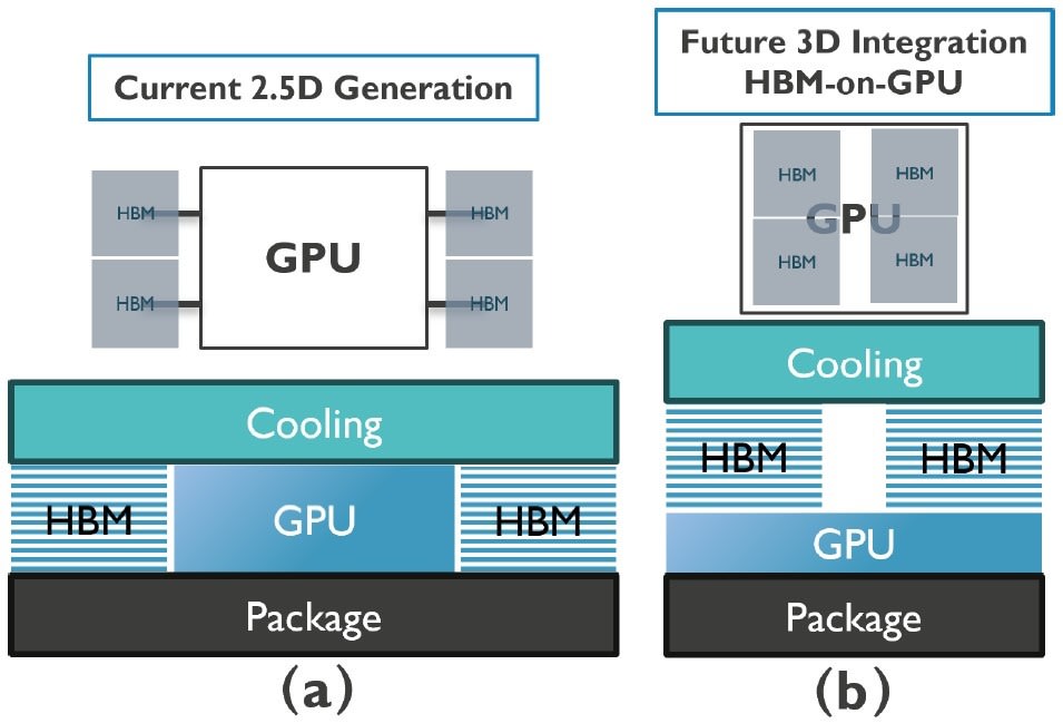
Why 2.5D HBM Packaging Can’t Scale Any Further
The limitations of the current 2.5D GPU designs are quite easy to spot once you look at how the hardware is physically arranged. In the current generation, HBM stacks sit around the GPU on top of an interposer, which is arrayed on two of the four edges of the GPU. This kind of layout has been pushed about as far as it can go from a design standpoint. Each stack of HBM essentially eats up a routing area and shoreline, which blocks direct other IO connectivity, such as GPU to GPU connections.
More critically so, restricts how many compute tiles can be placed upon a single package. Even NVIDIA’s largest multi-die accelerators still operate using this design constraint, because the interposer, not the silicon, basically limits the amount of scaling that can be done on a single package.
As in 3D variation, Figure 1b in the paper, stacking the HBM gives gives more headroom to future scaling. The memory stacks are more vertically aligned with the GPU die, which sits at the center of the package. Moving HBM directly on top of the GPU does clear up the perimeter of the die for more IO, thus enabling closer multi-GPU connectivity and collapsing the distance from the HBM stack to the GPU tile to practically zero.
Perhaps the biggest issue with this kind of design when moving to a 3D stack is it thermally breaks down quite quickly. Stacking four 12-high HBM stacks, which for current HBM3e would be around 4x 25W = 100W idle, 150W at load, on top of a -400W graphics tile, creates a thermal nightmare, Instead of spreading heat, it boils our shiny rocks.
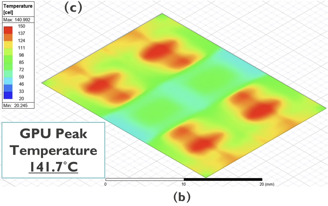
Using the same cooling methodology as the 2.5D scenario, the simulation yields a GPU temperature of 141.7ºC. If this was the final answer, good luck.
“Spontaneous GPU Combustion?!” – some person prepping a fire extinguisher.
As it stands in its raw form, the design isn’t remotely viable for use. Most electronics are specified for 105ºC, or 95ºC in controlled environments. This is do with both longevity, such as negative effects and electromigration that occur faster at higher temperatures, but also other factors such as expansion coefficients of large chips could warp substrates over time, causing defects. A modern datacenter is happy with 70ºC, not 140ºC. Even with the aggressive cold plate-based cooling, the 3D stacked HBM essentially acts as vertically stacked insulators which traps heat in the silicon behind it. In the data, the HBM stacks themselves only fare marginally better, but with elevated and uneven thermal gradients expected across the memory.
How to Cool a 3D GPU Stack on Fire
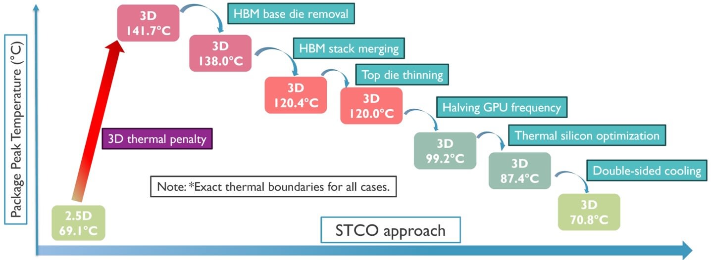
imec’s mitigation strategy, which is outlined in paper with the above illustration, points to a roadmap of how far the baseline 3D design can be relatively managed. imec calls this a combined STCO and DTCO strategy – system technology and design technology co-optimization, or XTCO for short. The problem is, when we’ve spoken with peers about this route to a more thermally viable solution, there was a lot of laughter. Let us know when you got to the funny part.
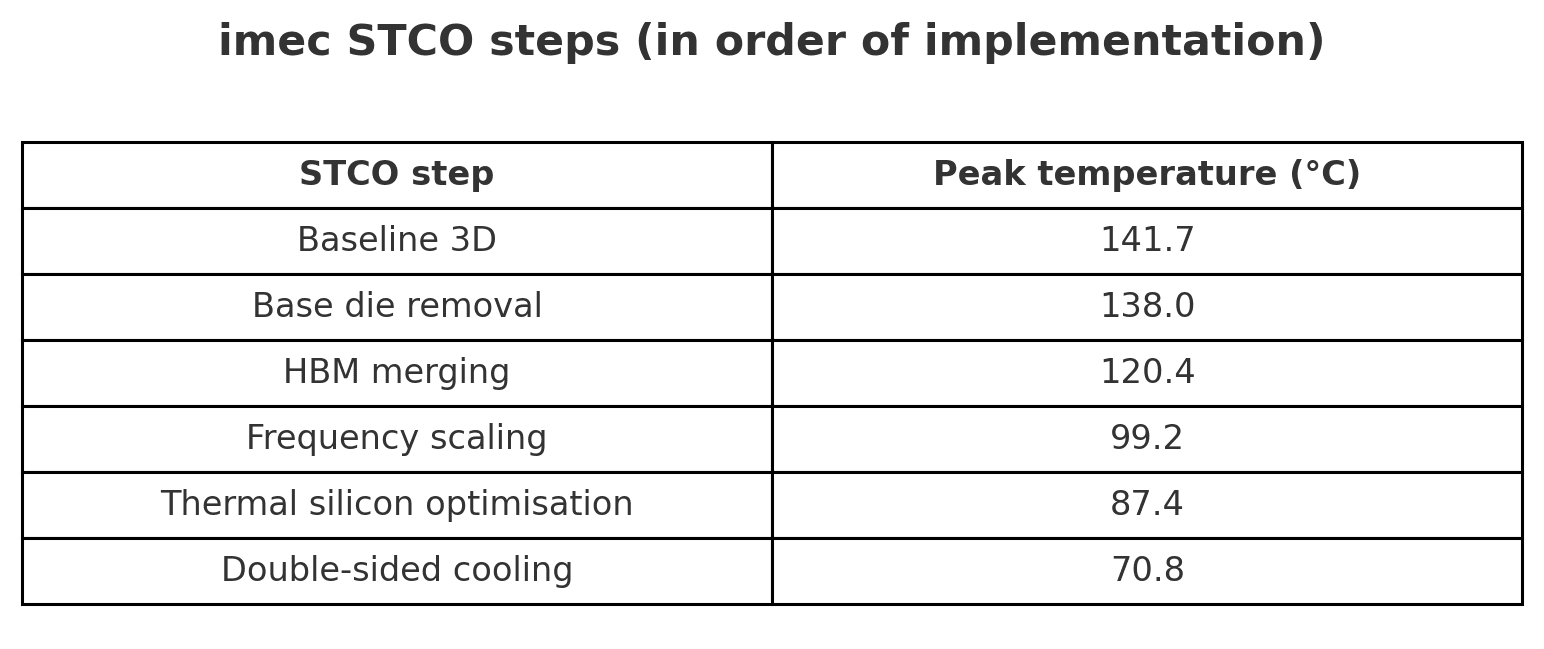
All in all, there are three main steps that claim to save around 20ºC each, plus a couple of minor ones.
Solution Part 1: Optimize the HBM
Looking at how each step of the STCO sits within imec’s roadmap, the first intervention is HBM base die removal. HBM is stacks of memory, but underneath is often a logic die specifically there to deal with the memory in terms of access patterns, longevity, and all the fun admin stuff that the memory controller on the accelerator shouldn’t need to worry about. In this solution, because of the 3D nature, imec proposes throwing the base die away and building it into the accelerator natively.
The paper doesn’t state whether this is built on top of compute transistors or anything, but removing it trims temperatures by a modest 4°C. It’s worth noting that no commercial HBM today ships without a base die, and future HBM4 and beyond is requiring custom base dies with more control to help deal with faster bandwidth and more memory. So cutting it out completely requires a custom design implementation, which might be feasible for the larger hyper-scale customers or those using design ASIC services, but not so much when it comes to general customers.
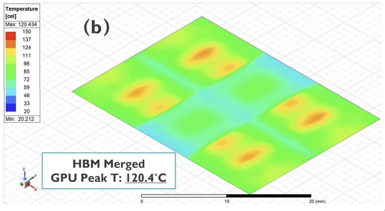
The next step in HBM targets the compound between the adjacent 3D HBM memory stacks. Molding between stacks is an ineffective and pretty poor heat spreader, and given that four stacks are implemented, this makes it even more redundant, even though it’s a necessary step. imec replaces this material by creating a merged HBM stack in a lateral manner. What we end up with is a double-wide HBM stack, which also requires the memory manufacturers to fundamentally change their design.
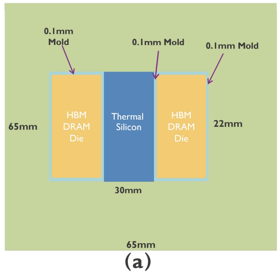
There’s a lot packed into this change, from the commercial nature of double wide memory with yields, to the supply chain. But according to imec it provides the first meaningful drop in thermal headroom; from 138°C to 120.4°C. This wouldn’t be an easy step to implement in volume, but not impossible if the industry was to bulk move to double wide HBM.
Top die thinning is next, and essentially what it says in the tin – a method of thinning the HBM stack, but within imec’s analysis, it barely plays a part in moving the needle towards a viable design. Cutting the top die thickness from 169um down to 41um, presumably using something like CMP, brings temperatures down by less than half a degree at 0.4°C.
Solution Part 2: Half the Frequency of the ASIC
Perhaps the biggest caveat, implementation, step, option, insert whichever terminology fits your opinion, is by halving the GPU frequency.
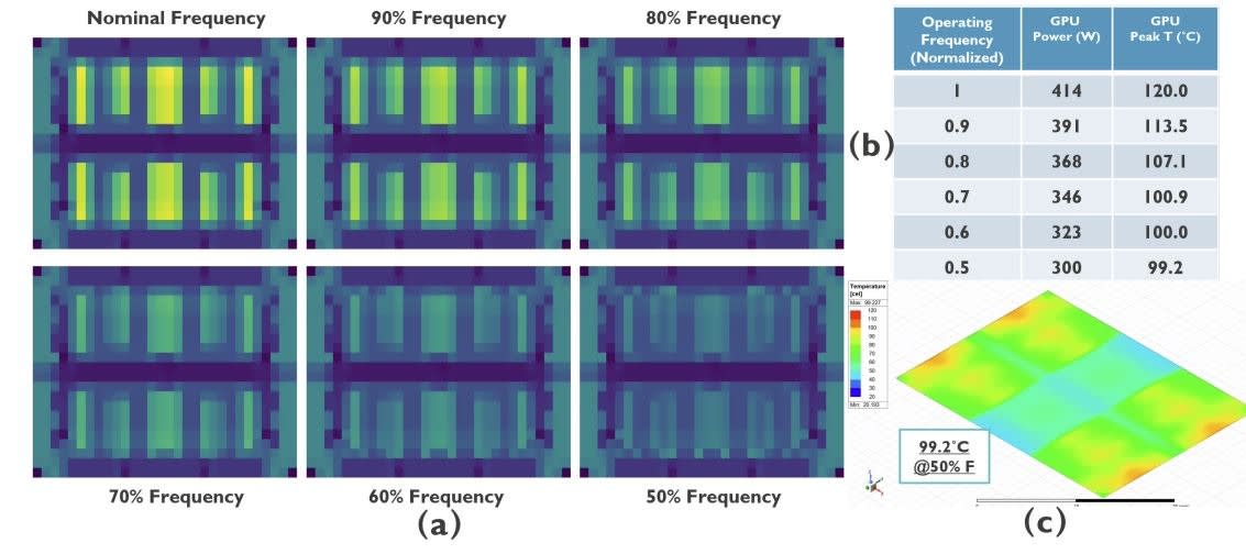
As imec acknowledges, by cutting GPU core frequency to 50% of the original value (without taking into account variables such as voltage scaling), the total power output of the GPU die drops from -414W down to -300W. This step reduces the peak temperature down from 120.4ºC to 99.2°C, making it the most effective step.
But it’s this step is where we start to see system-level trade-offs start to appear, as halving the frequency naturally reduces the overall raw compute throughput; this is a large amount of performance to lose from a baseline 3D HBM GPU design. We’ll get to this in a bit and why imec says that’s not so much a problem. (It is.)
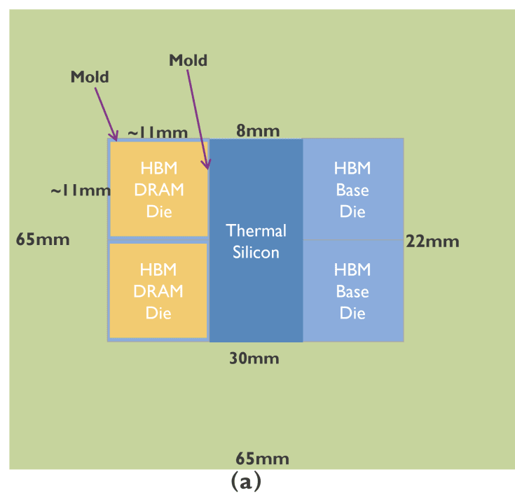
Moving on, the next stage is simply described as ‘thermal silicon optimization’, which, when taken on just face value, is a very vague use of terminology; it sounds good, but what does it mean? Something fancy, like co-design of GPU hotspots and memory above it? Actually no, it’s rather basic I’m afraid.
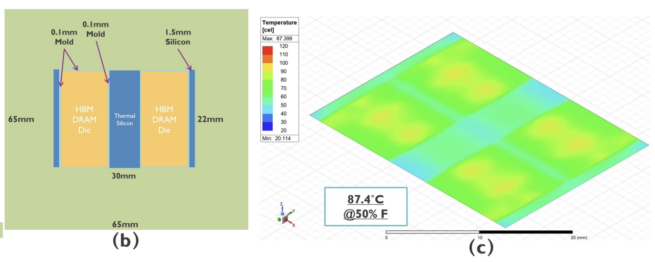
imec’s noted that the edges of the design were a source of hot spots. By placing spacers and shims of ‘highly conductive blocks thermal silicon’ above the hotspots (where it states 1.4mm silicon in (b) above), imec states it creates vertically adjacent pathways designed for heat to escape. This goes beyond relying solely on a centrally applied thermal silicon layer, which is present in the baseline design.
Solution Part 3: Changing the Cooling
We already covered the baseline cooling design that imec was using for its 2.5D layout and all of the 3D variations to this point. The last real stage in the process is to up the cooling. That baseline was already extreme for liquid cooling, but now in order to improve the situation, imec is suggesting more efficient, double sided cooling. Simple, just cool the ASIC from both sides.
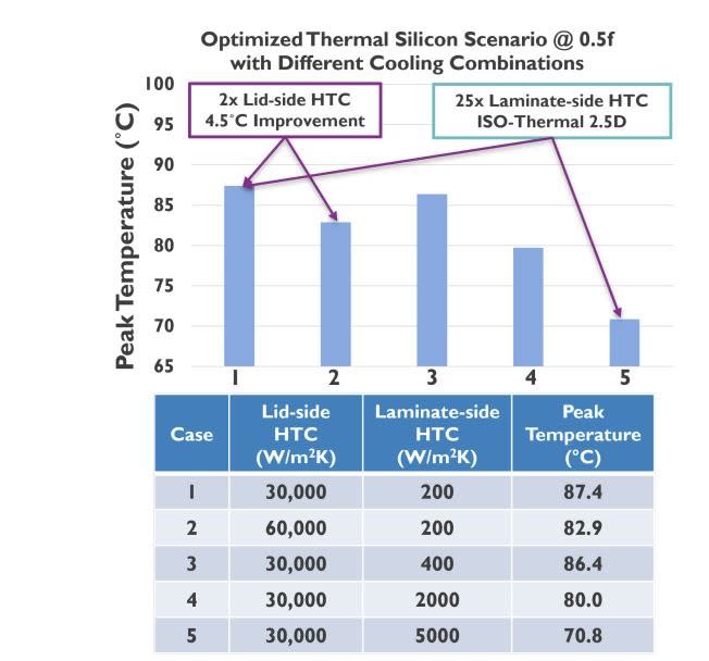
After the thermal silicon optimization, we’re on Case 1 in the table above at 87.4ºC.
Case 2 theorizes single side cooling, but more efficient heat transfer (60 W/cm2 per degree). I assume this means using a jet engine to force liquid through a loop.
Case 3 instead goes back to ‘regular’ chip cooling, but puts more cooling on the rear or ‘laminate side’ of the chip. Going from 200 to 400 is likely just a bigger heatsink and some faster air, but as a result it doesn’t move the needle much, only a degree from Case 1.
Case 4 and 5 just amp up the laminate side cooling, now going to liquid and good liquid cooling. With all this heat transfer, it means temperates come down a fair bit (as one would expect). However, the devil is in the detail – this is just a number put into the simulation.
But overall, looking at imec’s baseline implementation of 3D stacked HBM directly onto the GPU, it illustrates a necessity for backside cooling in some form, whether this is from the use of more advanced substrates within the heatspreaders, or even to more aggressive methods such as liquid-cooled baseboards. This is a huge signal in the design constraints of 3D integration, where it’s not just the packaging that is reshaped, but the entire cooling ecosystem surrounding it.
(Almost) All The Steps Are Required
Taking all of the steps in tandem and implementing them all on a whole shows that there is no single fix that makes 3D HBM on GPU thermally viable for use.
It isn’t until all the steps in imec’s STCO optimization strategy that we come to the levels of parity compared to 2.5D designs currently in use.
But the biggest step by far is halving the GPU frequency. We have some issues to address here.
The Performance Trade-Off
imec argues that much of the performance lost from knee capping frequency in half is offset by the increased memory throughput. imec shows that the GPU frequency has to be cut to accommodate the thermal challenges; in fact, cut to around half the frequency, which seems a little bit of an oxymoron. Sure, Occam’s razor dictates the simplest explanation is usually the one to go for, but many will be skeptical about essentially halving the overall performance of the GPU to its default or base settings.
The research paper gave the following data, which we’ve put into a slightly different format for readability. It’s a bit dense, but let’s walk through. On the vertical axis is performance, and on the horizonal axis is frequency, with ‘full’ frequency on the far left. The workload is a GPT-175B parameter training run, described as a ‘multi-head attention’ machine learning workload, which is more memory bound than compute bound.
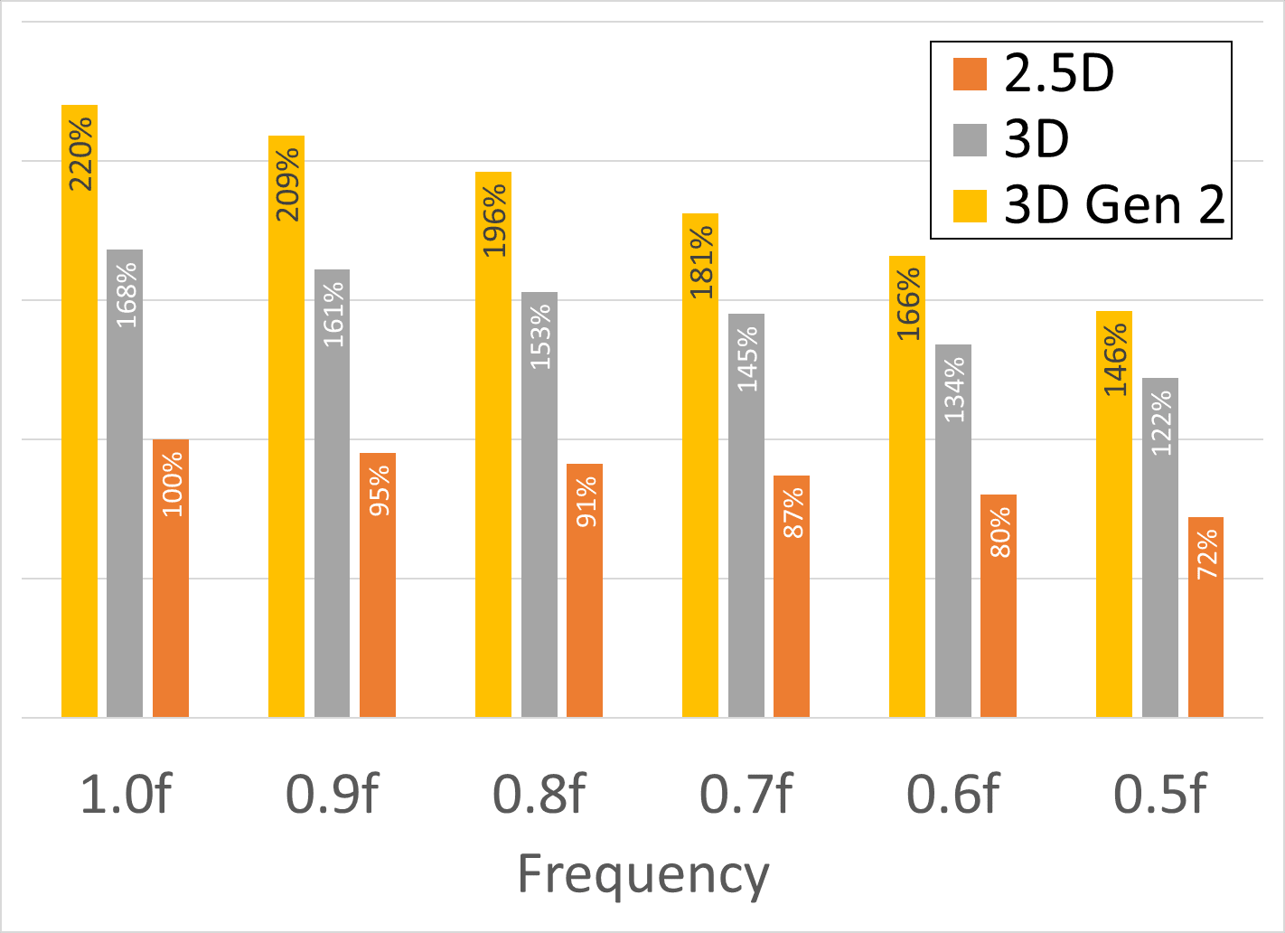
The orange bar is the performance of the 2.5D solution. That’s our base 100%, and we can see that as the compute frequency decreases, performance is lost, down to 72% when we’re at half frequency.
The grey bars are the new 3D model as we’ve outlined so far. If it was running at full frequency, then the chip would be 68% faster. But that’s at the 142ºC temperature, so as we decrease the frequency to half to make it viable, imec states that the performance of the chip is still +22% over the 2.5D design at full frequency.
The yellow bars are a ‘generation 2’ version. In generation 1, the 3D model assumed that the memory bandwidth in both 2.5D designs and 3D designs were equal – ie bit-widths and frequencies. The Gen 2 data assumes a 4x memory bandwidth increase over Gen 1, which imec says is ‘anticipated’. It doesn’t say how. But overall, while this line would give 2.2x the performance of our baseline at full frequency, it gives +46% at half-frequency. (That’s comparing full frequency 2.5D to half-frequency 3D Gen 2.)
So one question comes about, is it worth doing all this for a 22% or 46% performance increase?
Feasibility Meets Industry Reality
Even though the paper is short, it does imply major sweeping changes in the industry in order to be realised.
-
HBM
The idea of shipping HBM without the necessary base die sounds pithy and straightforward in paper, but in practicality, it requires memory vendors to redesign core parts of the product stack for, say, a specific customer, or even a specific product. We’re going to see how flexible the market is when HBM4 comes around and the first players use custom base dies, but the whole point of DRAM and HBM is that it’s a bulk commodity process. For 3D HBM-on-Logic, it now becomes an even more case-by-case basis, and only for those with the co-design integration. Merging the 3D stacks would be big, as the stacks would yield lower based purely on size. If we’re then embedding silicon bridges within to replace the base dies, then it will increase the demand on packaging lines, and there are not many facilities currently set up across the globe that could even to implement these design characteristics, let alone produce with a high enough yield to prove viable. It would be a multi year effort.
-
Frequency lol
Taking a shotgun to GPU frequency and blowing half of it off the spec sheet is a crazy proposal. While it is a thermally convenient step in terms of viability, but it does trade raw compute for thermal headroom, it puts much of the weight of performance on memory-bound AI workload situations. What about for other workloads?
The problem is that customers won’t want to hear that the new chip is half the theoretical peak performance than the old one, oh and it’s going to cost a lot more because of the complex packaging and cooling. Just the raw FLOPS getting cut in half isn’t a winning marketing strategy. Sure, the workload numbers in some cases goes up, but then it becomes a memory optimized SKU for specific verticals, not the catch-all that most transformer AI accelerators are aiming at today in the datacenter.
-
Can you pick and choose?
imec’s paper reads like a recipe – something that requires all the parts to participate to get the result. Three big changes to reduce the thermals – and some of those changes don’t really have answers. For example, take the dual side cooling – while top-side cooling was ‘looked at’, could we consider intra-chip cooling? Or perhaps given the market is talking about High-Bandwidth Flash as a co-point to HBM, perhaps that is more thermally efficient? When we saw this paper, we were shocked about how potential high-impact it would be. But +22% on certain workloads given all the caveats in yield, supply chain, and cost? It’s good that the research was done, but the results don’t feel too convincing.
Conclusion: A Roadmap, Not a Product
This research shows that the future of HBM is far from settled. There’s a line of interconnect research that’s looking at having 2.5D HBM but enabling two modules deep, rather than just one. Celestial AI (recently acquired by Marvell) and other optical interconnect companies are talking about replacing HBM with an optical connection to a memory appliance, providing multiple times the bandwidth and capacity by having the HBM in a different server, rather than in super close proximity.
The huge obstacle of thermals in 3D HBM-on-logic, without modification, kills the baseline design stone dead. But engineering through a full stack of refinements, cooling adjustments, and oh, just sacrificing just 50% of raw GPU frequency to make it viable, is going to require a lot more than simply stacking HBM on top of the GPU die.
What imec has offered up is a roadmap to the viability of 3D HBM on die, not a product per se. It’s a signpost in the road that points towards a future of where performance scaling relies less on just transistor count, raw frequency, and more effectively the industry can pivot and learn to manage heat within the third dimension. From a philosophical standpoint though, without the right marketing, I doubt anyone is going to go on stage and talk about halving the raw throughput on their chip.
A more grounded takeaway is that imec’s modelling exposes which parts of the current GPU–HBM stack are likely to become the next bottlenecks as AI systems scale. The thermal limits identified here are not unique to this configuration – they point to broader pressure on power density, heat extraction, and memory placement as accelerators continue climbing past hundreds of watts or even thousands. Even if 3D HBM on-die never ships due to economics or scale, the constraints highlighted indicate how aggressively vendors are going to pursue denser multi-tile layouts, larger HBM footprints, and more compact packaging geometries, all of which we’ve started to see from foundries, design teams, and hearing from executives.
Source: imec, IEDM 2025 Session 17-3