
Five things you need to know before reading:
-
Both Samsung and SK Hynix have working LPDDR6 silicon. Just seven months after the JEDEC specification was ratified.
-
The effective bandwidth at 14.4 Gbps is 38.4 GB/s per die.
-
SK Hynix chased bandwidth, Samsung chased efficiency.
-
The shmoo plots tell the story on where the silicon is right now.
-
This is just the first generation of LPDDR6 silicon. It’s only round one, more to come
What Samsung and SK Hynix have disclosed in individual papers published at ISSCC 2026 shows that both companies have working LPDDR6 silicon, despite the standard being ratified by JEDEC only a few months ago. As progress marches on, recent ML workloads have created a demand for high capacity, high speed memory, with throughput bottlenecked in all sorts of devices. In small devices such as smartphones and notebooks, it means the memory subsystem is one of the biggest limiting factors in creating devices to run capable and up-to-date on-device models.
What both companies showed off at ISSCC 2026 is more interesting than it looks on the surface. While both Samsung and SK Hynix arrived with working silicon, they made fundamentally different decisions about where to target its respective designs and optimizations. Samsung outlined a more modest approach to speed and bandwidth, trading pure performance for power optimizations in various ways. SK Hynix, however, leveraged its newest 1cnm process node to push straight towards the 14.4 Gbps ceiling as outlined per the JESD209-6 spec. Together, the two papers give us the first detailed, independently verified look at how LPDDR6 actually behaves in silicon rather than just on paper.
The current LPDDR Family in Brief
LPDDR5 originally debuted in 2019 with a peak data rate of 6,400 Mb/s per pin, which is roughly double that of LPDDR4X. LPDDR5X followed suit in 2021 with a peak data rate of 8,533 Mb/s, then SK Hynix managed to push things to 9,600 Mb/s with what became known as LPDDR5T. Samsung eventually went one step further and validated LPDDR5X at 10,700 Mb/s on 12nm for the Dimensity 9400 platform. The table below shows the generational uplift in peak data rate and bandwidth per die from LPDDR4X all the way up to the current LPDDR6 memory.
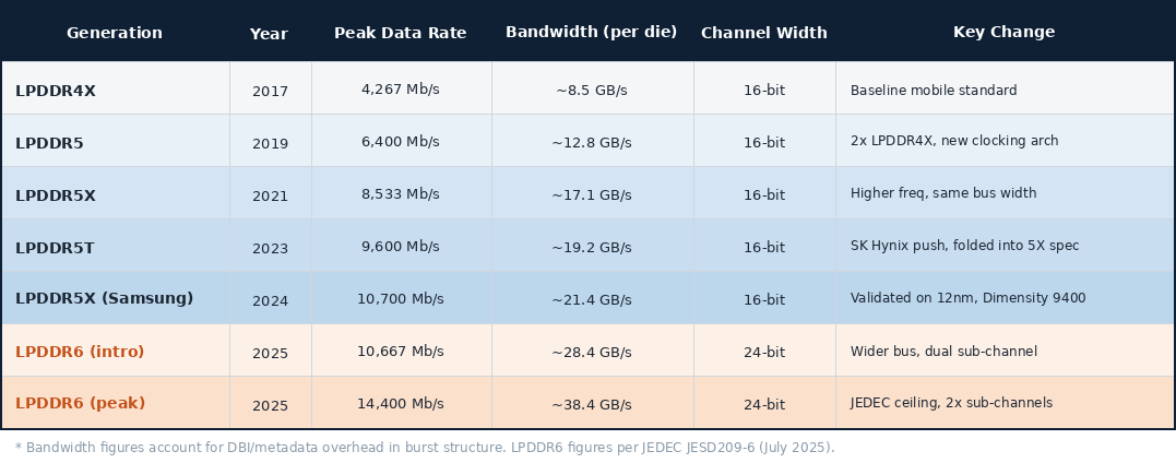
Throughout all the generations listed above (LPDDR4X to LPDDR5X) all use a 16-bit channel, which essentially meant that the connection between the memory and the processor was the same width regardless of how fast the data rate rose. LPDDR6 changes this to a wider 24-bit channel, which is arguably more important than just the speed itself, as it means it will be difficult to build a unified controller that supports both LP5 and LP6 modes.
LPDDR6 organises its 24-bit channel as two 12-bit sub channels per die, and this has implications in how the memory actually operates. Each 12-bit sub channel handles its own data independently from the other, and gives the memory controller more flexibility in how it handles requests and allows smaller access granularity of 32 bytes per sub channel (down from 64 bytes in LPDDR5). For AI workloads that generate lots of smaller and typically irregular memory requests rather than large sequential ones, it means random memory access should work more efficiently, and thus theoretically spends less time fetching more data than the workload actually needs.
LPDDR5X bandwidth was becoming insufficient for newer AI workloads being planned for mobile devices, and the combination of the higher data rate and wider bus width directly addresses this. Running capable on device AI models requires the memory subsystem to move large amounts of data quickly and consistently, and LPDDR5X at 8,533 Mb/s (16-bit) delivers around 17 GB/s of peak bandwidth per die. LPDDR6 at its peak with 14,400 Mb/s across a wider 24-bit channel delivers up to 38.4 GB/s per die as confirmed by SK Hynix’s ISSCC 2026 disclosure. This is roughly a 2.25X improvement over LPDDR5X and more than 3X over LPDDR5.
Before moving on, let’s familiarize ourselves with what JEDEC specified last year with its JESD209-6 specifications.
What the JEDEC Actually Specified (Published July 2025)
The official JEDEC JESD209-6 specifications define a peak data rate of 14,400 Mb/s per pin, with an introductory grade starting at 10,667 Mb/s, but there’s more to things than just peak data rate. Effectively, the peak bandwidth lands at 38.4 GB/s per die as SK Hynix disclosed, rather than the 43.2 GB/s theoretical maximum you get from multiplying the data rate by the bus width.
Beyond bandwidth, LPDDR6 makes on-die ECC mandatory rather than optional, unlike LPDDR5X. This means that error correction is now performed within the memory array before the data reaches the processor. LPDDR6 also introduces Per Row Activation Counting, which defends against Rowhammer. Rowhammer is a well-documented memory vulnerability where repeated access to the same memory row can corrupt the data of adjacent rows. In addition, a new dynamic efficiency mode reduces the interface to a sub-channel during low-bandwidth operation, providing distinct power-efficiency benefits critical for mobile devices.
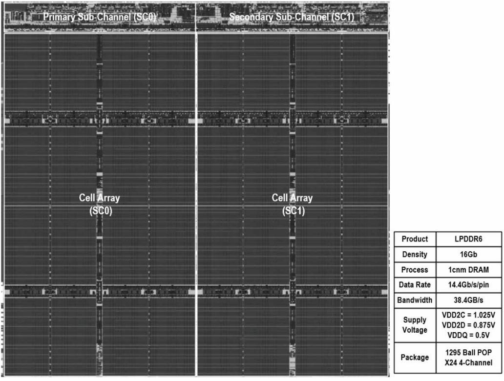
SK Hynix at ISSCC 2026: 16Gb LPDDR6 on 1cnm (Paper 15.7)
SK Hynix presented its 16Gb LPDDR6 at ISSCC, using 1cnm, the latest generation of its 10nm-class DRAM family. The headline numbers are confirmed directly from the die micrograph summary table in Figure 15.7.7: 14.4 Gbps per pin, for a total bandwidth of 38.4 GB/s. The chip runs on two separate voltage rails: a higher one for speed-critical data and a lower one for everything else. This is a key part of how SK Hynix manages power consumption across different operating conditions.
More distinctly, the chip itself is operating at two different voltage levels. The higher-voltage rail, VDD2C, is running at 1.025V, while the lower-voltage rail, VDD2D, is operating at 0.875V. The VDD2C is the critical part, where more power is needed to deliver that maximum bandwidth of 14.4 Gbps per pin, while the VDD2D is designed to handle everything else.
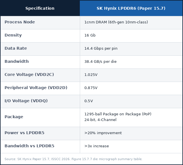
SK Hynix is claiming over 20% better power efficiency and higher per-channel bandwidth compared to LPDDR5. Running different parts of the memory chips at different voltages is a precise way to squeeze out additional power efficiency, but SK Hynix also claims a 3X increase in bandwidth over LPDDR5.
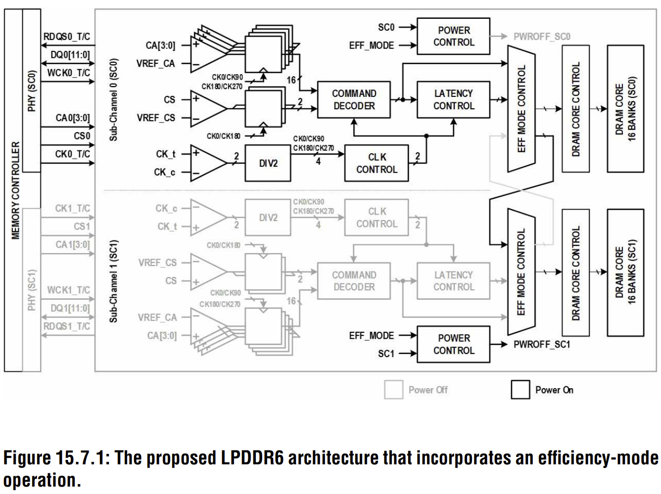
The architecture diagram above (Figure 15.7.1) provides a clearer picture of how the dual sub-channel design operates day-to-day. SC0 is the primary sub-channel, which has all of the active logic running, and SC1 mirrors it. However, in efficiency mode, the entire secondary block is powered off, with SC0 taking full control of all 32 banks. In that particular state, running at 12.8Gbps across a single sub-channel, standby current drops to 87.3% and operational current to 81.1% of normal mode. Realistically, this is the state the device spends the vast majority of its life in, which means those numbers arguably matter a great deal more than the peak figures do.
Much of what SK Hynix provides in this paper focuses on managing power at the ends of the speed range rather than simply at its peak. The CA (command and address) bus, which is responsible for telling the memory what operation to perform and where to perform it in LPDDR6, operates between the frequencies of 1.6 GHz and 3.6 GHz, which is roughly triple that of LPDDR5, as cited by SK Hynix, and this creates some real challenges in multi-rank configurations where CA pins are shared between dies.
To address this, SK Hynix splits the operating range into three frequency bands, each with its own dedicated buffers, which are selectively activated based on operating conditions. Combined with a fast CS control scheme that gates CA signal paths more efficiently at lower speeds, standby current drops by 42% at low frequencies and 19% at mid frequencies. For a device that simply sits idle for the vast majority of its time, that is ultimately where most of the real power saving lies.
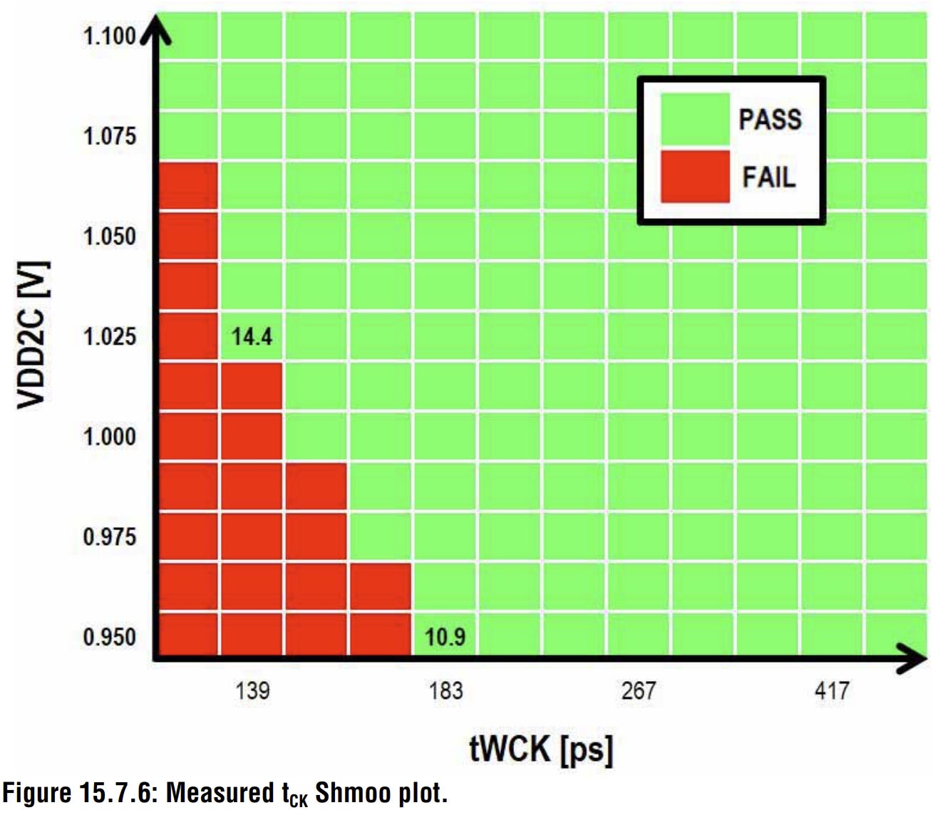
The shmoo plot in Figure 15.7.6 shows SK Hynix’s power and voltage targets for the data rate. For those unfamiliar, a shmoo plot is a visual representation of where a chip passes and fails across a range of voltages and clock speeds. This gives us a much clearer picture of where the silicon itself is actually comfortable operating versus where it is simply being pushed to its limits. At 1.025V VDD2C, SK Hynix’s device passes at 14.4 Gbps, which is also the JEDEC ceiling.
Dropping the voltage down to 0.950V causes the bandwidth to fall back to 10.9 Gbps. This says that SK Hynix’s 1cnm process needs that extra voltage headroom available to operate reliably at its peak speed without the performance dropping. Without this headroom, performance drops off pretty sharply. This is SK Hynix’s first generation LPDDR6, and this isn’t unusual for a new process node, but it does paint a different picture to Samsung, which opts to trade better power efficiency for lower bandwidth.
That voltage-to-speed relationship becomes particularly important when we sit this directly next to what Samsung showed in its paper, because the two companies made very clear distinctions about where to optimize, and their respective shmoo plots reflect that.
Samsung at ISSCC 2026: 16Gb LPDDR6 at 12.8 Gbps (Paper 15.8)
Samsung presented its own disclosure at ISSCC 2026, covering a 16Gb LPDDR6 device built on its 10nm-class DRAM process. The summary table in Figure 15.8.7 and the table below directly confirm the key specifications.
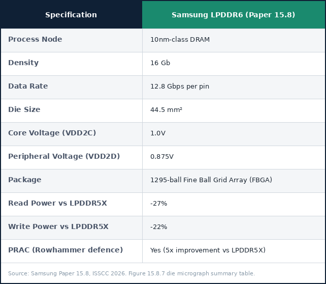
That 12.8 Gbps Samsung disclosed isn’t chasing the 14.4 Gbps ceiling in quite the same way that SK Hynix is. The paper itself describes 12.8 Gbps as the JEDEC-specified minimum voltage operating point, which shows that Samsung ultimately chose to focus its engineering effort with its first-generation device on power efficiency.
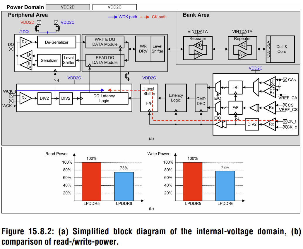
The power domain split shown in the above illustration (Figure 15.8.2) is central to how Samsung achieved its efficiency targets. Rather than running everything at a single voltage, Samsung splits its circuits across two supply rails depending on how speed-critical they are. Samsung routes the speed-critical circuits to VDD2C, with peripheral and non-critical circuits to VDD2D, which operate at 1.0 V and 0.875 V, respectively.
The bar charts in the same figure show the outcome fairly clearly: read power drops to 73% of LPDDR5X, and write power drops to 78% of LPDDR5X. The DQ pins are the physical connections on the memory chip responsible for the movement of data between the memory and the processor. At high speeds, these pins switch states rapidly and consume power every time a pin changes from 0 to 1 and vice versa. Samsung also extended power gating to the high-frequency DQ (data I/O) and claims it is cutting standby power by an additional 10%.
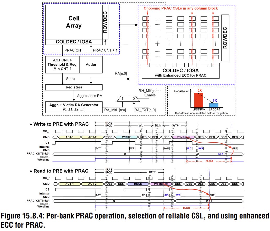
Samsung also implemented Per Row Activation Counting, which is more commonly referred to as PRAC, and this is Samsung’s deterministic answer to the Rowhammer problem. Rather than simply relying on probabilistic refresh schemes, PRAC embeds counters on a per-wordline basis directly inside the array itself, tracking every single row activation and triggering mitigation before the threshold for exploitation is actually reached. The bar chart in Figure 15.8.4 shows the results: LPDDR6 with PRAC requires approximately five times as many attacks before mitigation is triggered compared to LPDDR5X. For a standard that is moving increasingly into automotive and edge AI territory, that kind of deterministic protection matters a great deal more than it ever did in a purely smartphone context.
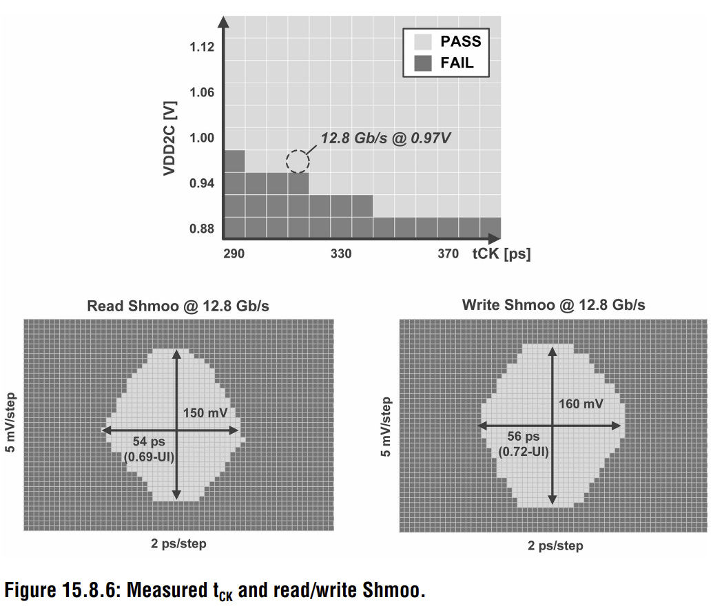
Samsung’s Shmoo plot in Figure 15.8.6 (above) highlights what the voltage choices suggest: it has optimized primarily for power efficiency over raw bandwidth. Looking more closely at the Shmoo plot, Samsung’s LPDDR6 reaches 12.8 Gbps at 0.97 V, suggesting the silicon isn’t being pushed to its limits.
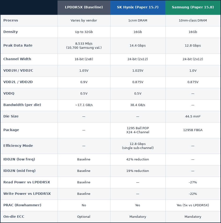
LPDDR6 at ISSCC 2026, SK Hynix and Samsung: A Direct Comparison
With Samsung and SK Hynix and its respective LPDDR6 designs, it’s worth noting that we can’t directly compare power efficiency. SK Hynix reported a 20% overall power efficiency compared with LPDDR5, whereas Samsung disclosed 27% better read and 22% better write performance compared to LPDDR5X. Both companies provide different metrics and baselines, which makes a direct comparison difficult here.
The table below pulls its figures directly from the two primary papers. Where data was not explicitly stated by either company, we have simply left it blank rather than filling in the gaps with figures from secondary sources.
LPDDR6 at ISSCC 2026: The Overall Picture
Both companies brought working LPDDR6 silicon to the stage, and both within just seven months of the standard being ratified. In addition, Samsung and SK Hynix are jointly working with JEDEC on the LPDDR6-PIM standard reported by TrendForce as of December 2024, which would integrate computational capabilities directly into the memory itself rather than relying on the host processor.
What both Samsung and SK Hynix disclosed at ISSCC 2026 gives us the first real look at its respective LPDDR6 designs and where they are currently focusing their efforts; SK Hynix on more bandwidth and Samsung on power efficiency. SK Hynix’s Shmoo plot shows voltage sensitivity on its first-generation 1cnm silicon. As the process matures, these margins will likely improve.
On process node maturity, Samsung’s 16 Gb die measures 44.5 mm², with a density of 0.360 Gb/mm². Samsung did not specify the specific node its LPDDR6 silicon is built on other than the 10 nm-class DRAM process. This could be 1a (1st gen), 1b (2nd gen), or 1c (3rd gen), with the 1c being the equivalent in SK Hynix’s 1cnm. SemiAnalysis concluded in their ISSCC 2026 roundup that Samsung’s LPDDR6 is more likely to be consistent with its 1b node than with the latest generation. The dual sub-channel architecture does add area, which partially explains the lower density, so a direct comparison of density with a single-channel design is complicated.
Each of the papers is well worth reading in full, but I expect both SK Hynix and Samsung to push further up the speed curve on their respective manufacturing processes. Both are first-generation LPDDR6 silicon, so the second time around could look very different.
Some Additional Thoughts
Section from Ian
In speaking with vendors at Computex 2026 this year about DDR6 and LP6, they stated that the difference between the two standards isn’t going to be as big as DDR5 and the LP5 variants, which may lead to unified designs across DDR6 and LP6 in silicon. While that doesn’t matter much for devices that will use LP6 anyway, it does mean that hardware that normally uses DDR might have an easy route to an LP6 installation depending on market volumes. One vendor said to me that it will really depend on whether DDR6 or LPDDR6 will hit the market first, and if there’s a lop-sided volume element.
But also, with the increased demand for CPUs and in general Arm CPUs using LP memory, we might see a shift also from the x86 vendors to an LP design at scale. For GPUs, AMD has already shown its next-gen AI chips in renders using both HBM4 and LP5X as a tiered memory hierarchy, just to add to the mix. Intel’s new Crescent Island AI inference PCIe card uses up to 480 GB of LP5X per GPU.
In terms of timeline, the DDR6 standard should be ratified this year, leading to first consumer products in 2027 and then ramping in the 2028/2029 timeframe. LP6 should ramp slightly faster than that. Normally with a memory transition we talk about the crossover point from one standard to another, usually driven by pricing. In today’s macroeconomic environment, all bets are out the window, and each of the memory vendors is simply trying to (a) make as much as they can and (b) offer something that off the shelf has a higher performance/density at 100% yield than their competitor. What’s driving the new standards is that the compute needed wants the performance, density, and power improvements.
In speaking to the memory vendors too, it’s no surprise that 2026 volume is sold out, 2027 is sold out, and it looks like 2028 is going that way fairly soon. It will be interesting to see that effect on the new generations of technology, if that’s a help or a hindrance. We have an upcoming interview with Micron later this week, so please stick around for that.