

For most of the industry, Fujitsu is recently synonymous with supercomputers — the kind that top the Top500, power national research labs, and rarely surface outside high-performance computing circles. But now, Fujitsu is preparing to return to its roots. Its next processor, Monaka, moves away from exascale benchmarks and toward deployment in scalable, conventional datacenter infrastructure. And it’s targeting wide-scale deployment in a market defined by hyperscalers, energy constraints, and Arm’s rising presence in cloud infrastructure.
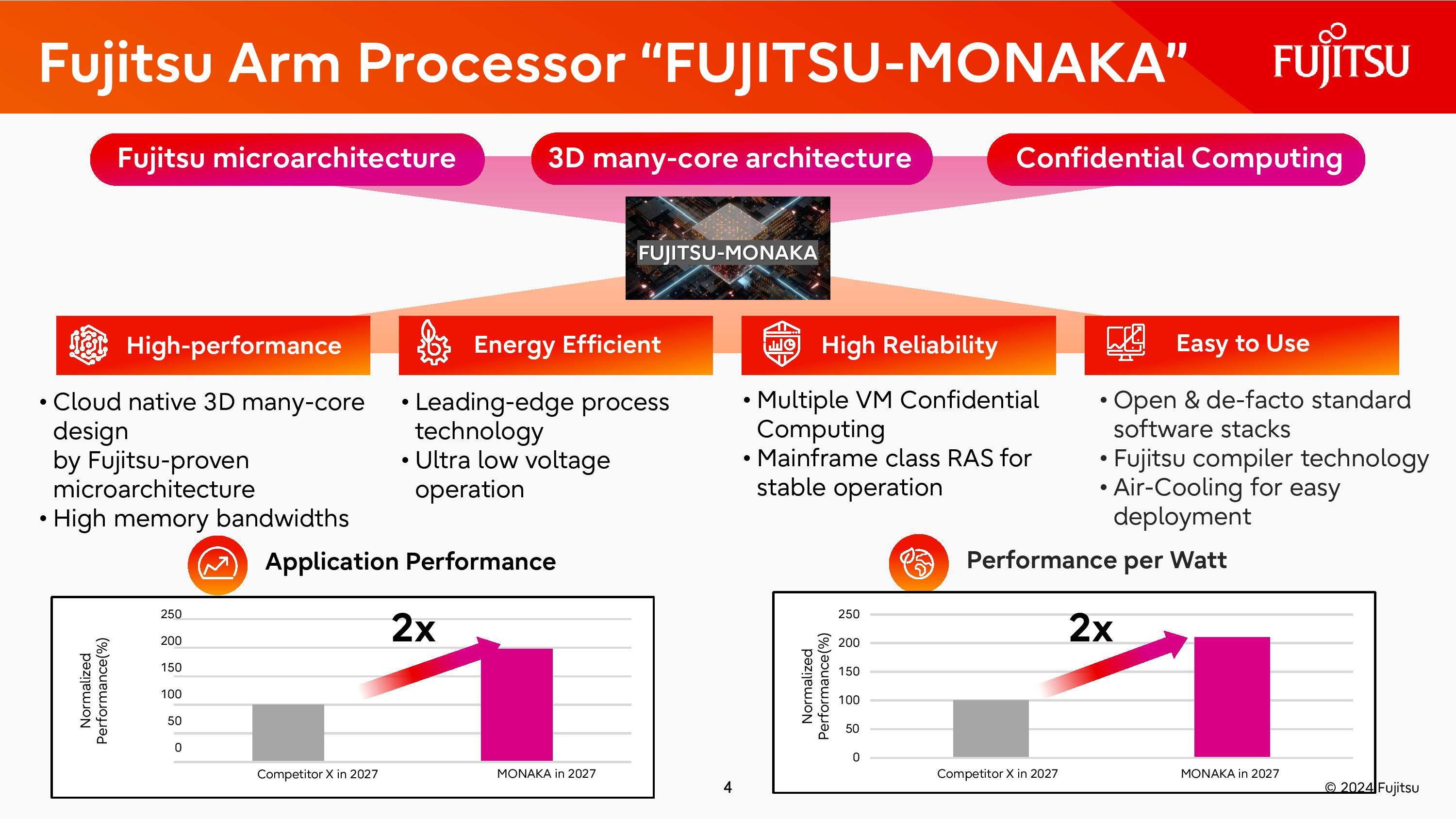
This marks a significant strategic shift. Fujitsu’s previous processor, the A64FX, was a technical landmark. It was the first Arm-based CPU to power the world’s fastest supercomputer at the time. But Monaka is something different – it’s built around a 2nm core die, arranged in a 3D many-core chiplet layout, designed for air-cooled servers, using regular memory, and optimized for confidential computing, ultra-low voltage operation, and sustainability at scale. In short, it’s designed to be a purpose-built, efficient, secure CPU for the future of cloud-native workloads — not just scientific simulation.
Monaka also reflects a broader national strategy. Its development is supported by Japan’s Green Innovation Fund, with funding and oversight from NEDO, the New Energy and Industrial Technology Development Organization. Fujitsu has described the goal as delivering next-generation processors for green datacenters, with performance and power targets aligned to Japan’s environmental policy. It’s part of a larger trend toward sovereign compute infrastructure – one echoed in similar efforts across the US, EU, China, and India – but with a distinctly efficiency-first philosophy.
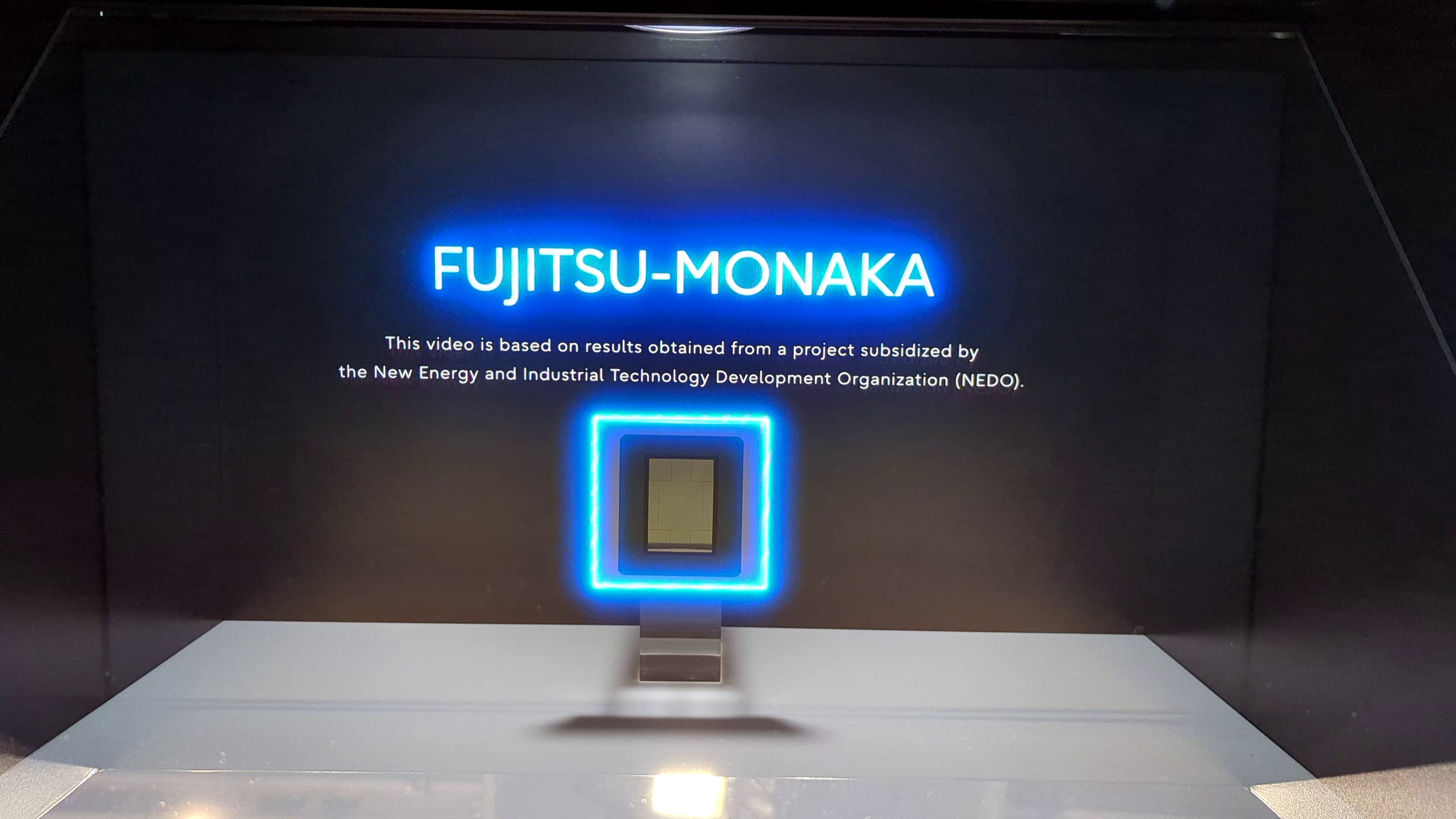
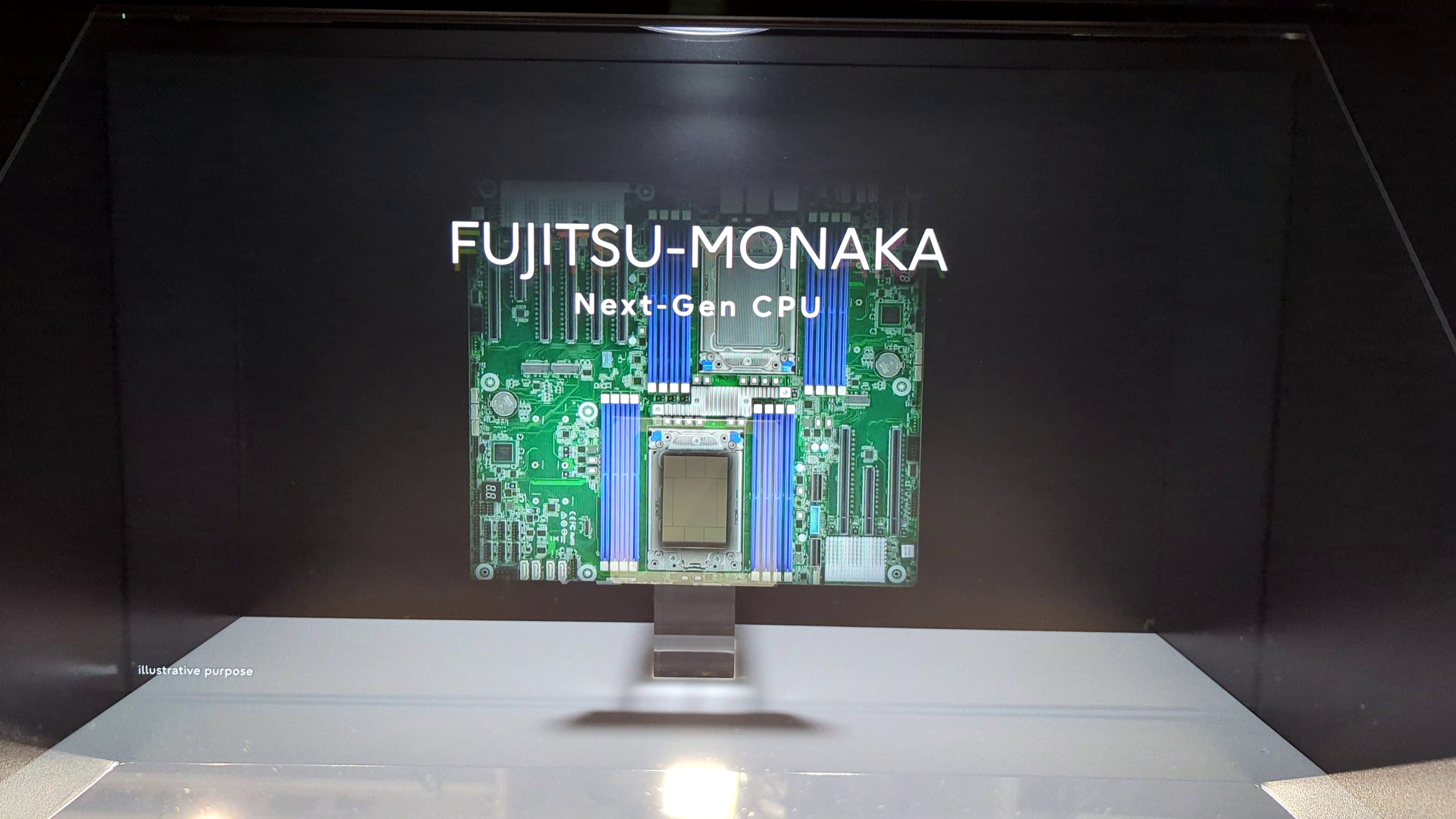
At this year’s Mobile World Congress in Barcelona, Fujitsu provided its most substantial update on the project to date. While Monaka was first announced in 2022, I first saw mention of it at the Supercomputing 2023 conference, and this was the first time the public saw a silicon mockup. Fujitsu also compiled its previous platform specifications. No stage presentation, no formal press event — just a quiet display behind glass, a looping animation, and a wall of internal slides.
But for those who’ve followed Fujitsu’s architectural lineage – from SPARC64 to the K-Computer to A64FX – the message was unmistakable. The chip is real. Development is progressing. And while Fujitsu may not be chasing attention, it’s absolutely targeting deployment.
Inside Monaka
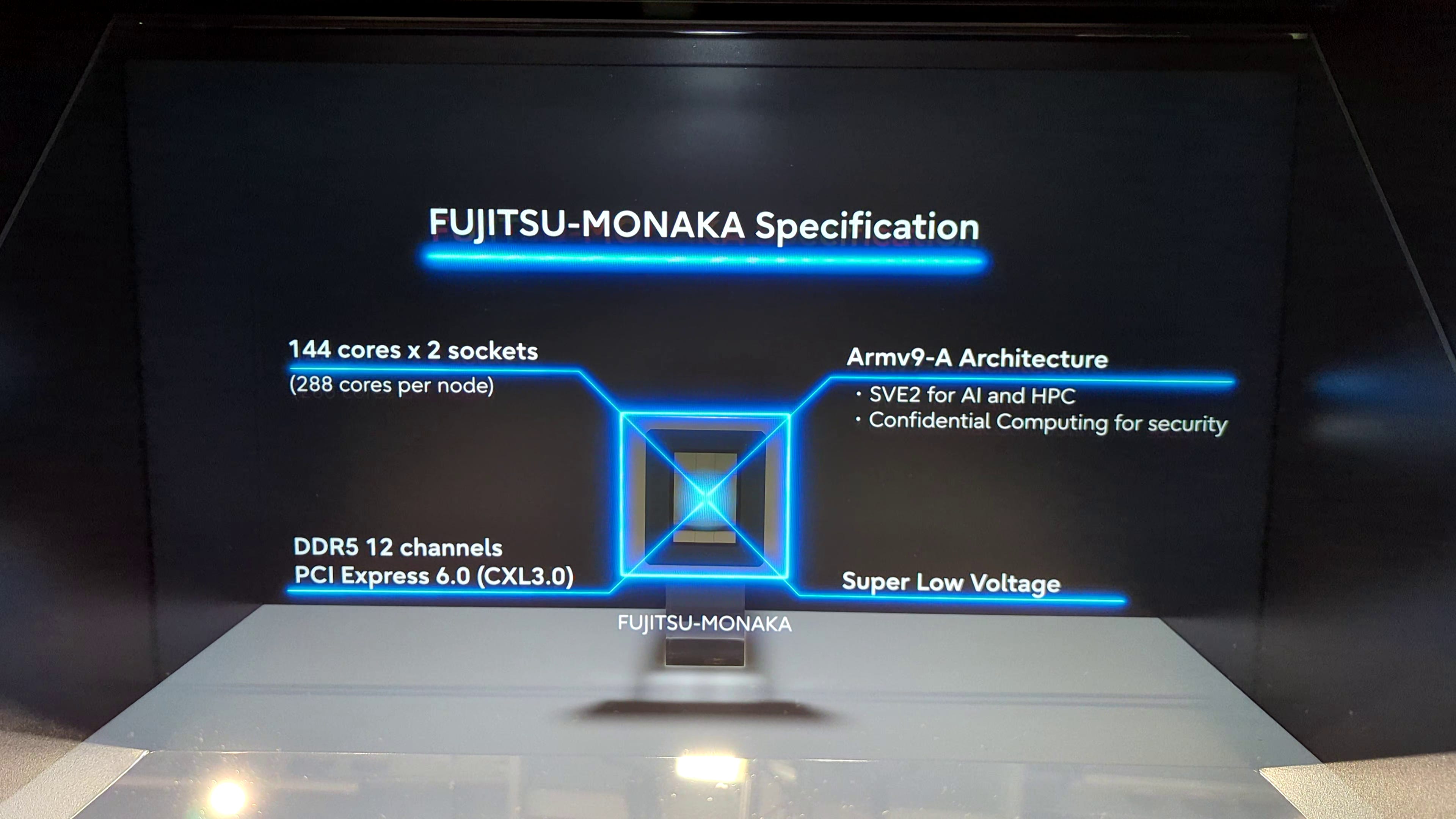
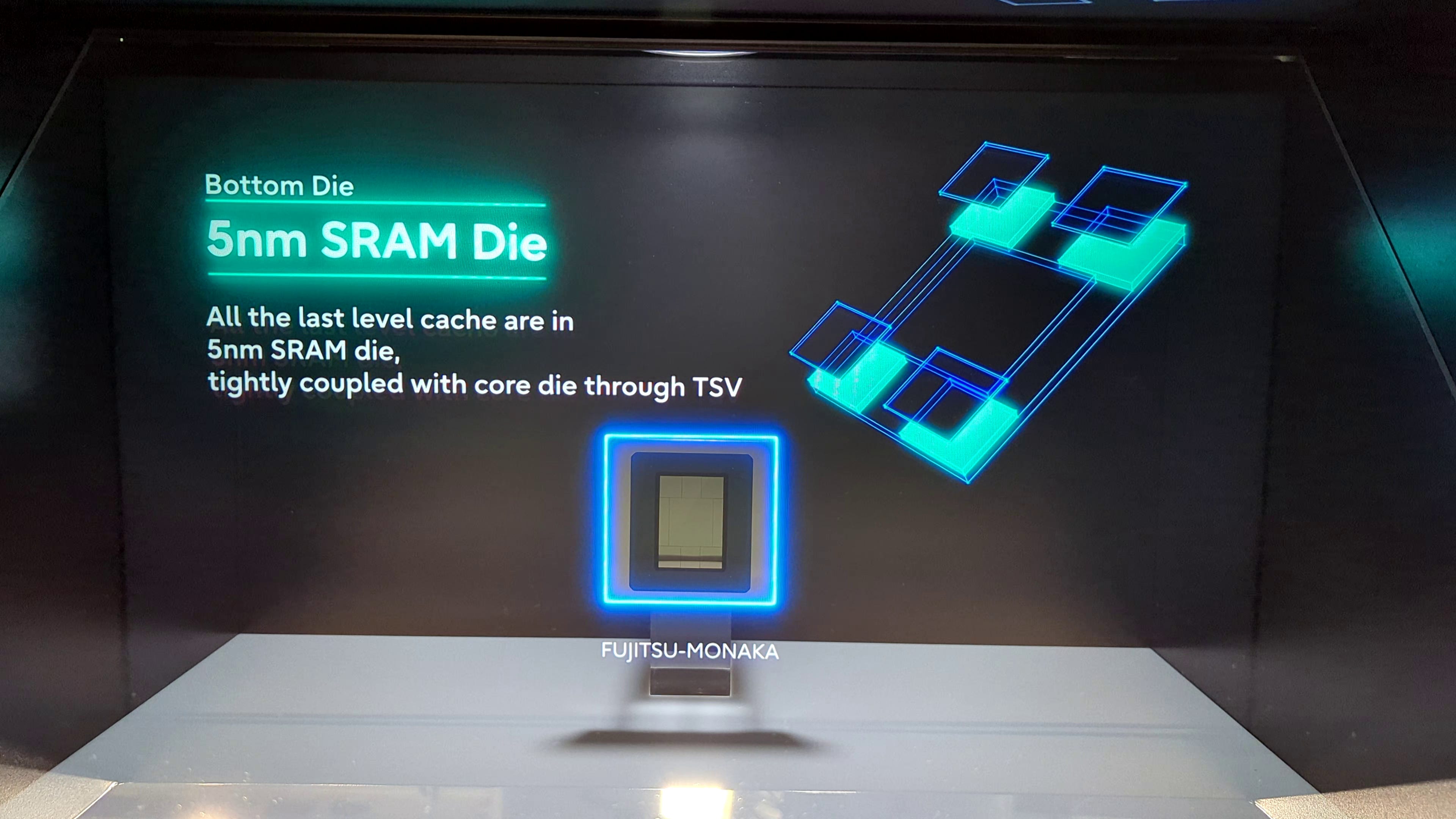
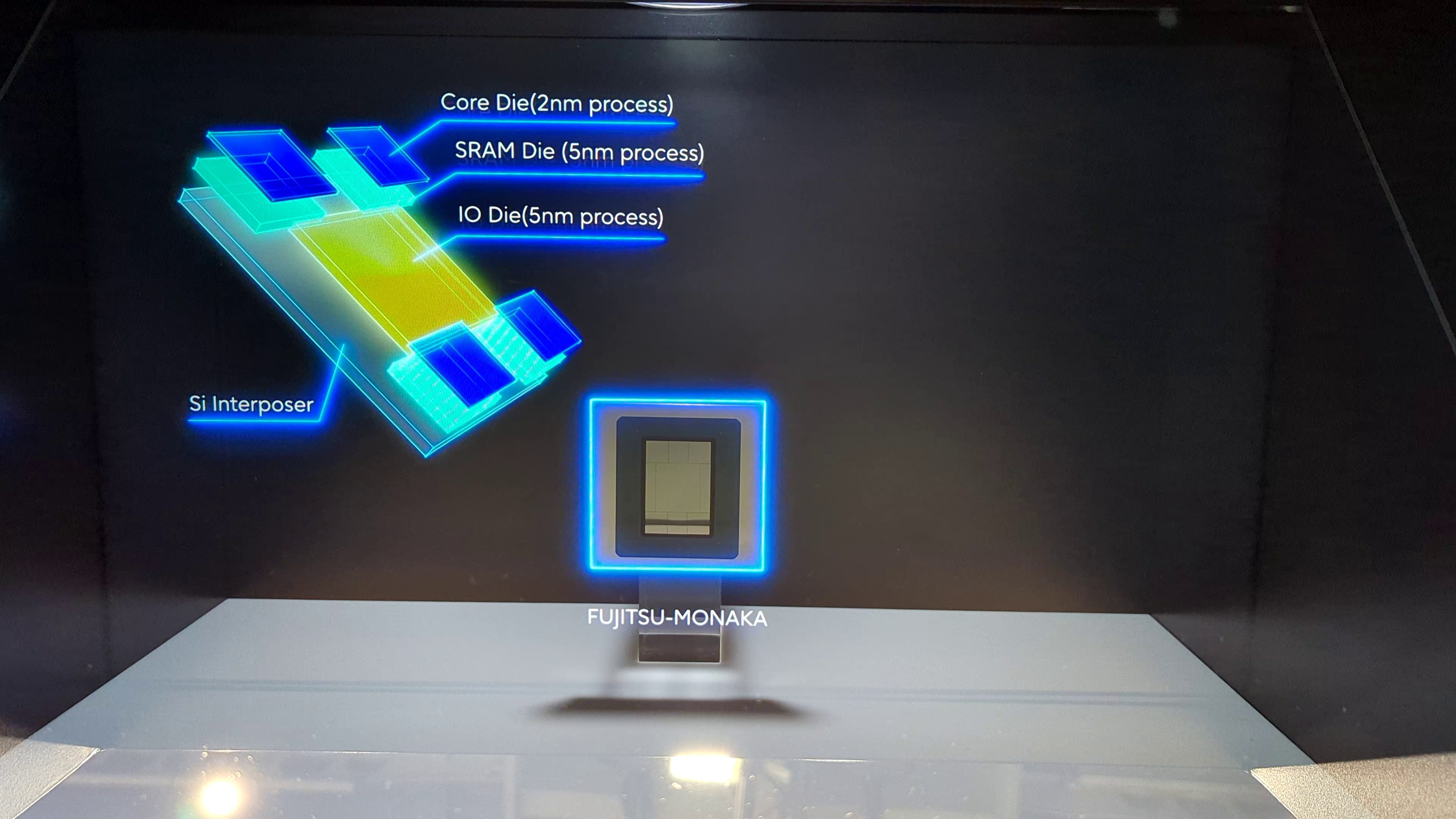
At the heart of Monaka is a 3D chiplet design that splits logic, memory, and IO across different process nodes. The core die is manufactured on a 2nm process, while the SRAM and IO chiplets use a more ‘mature’ but still advanced 5nm node. These are vertically integrated using through-silicon vias (TSVs) and mounted on a silicon interposer. In its planned dual-socket configuration, Monaka will offer 144 Armv9-A cores per socket, or 288 cores per node, and be packaged for air cooling and targeted at standard 2U datacenter servers.
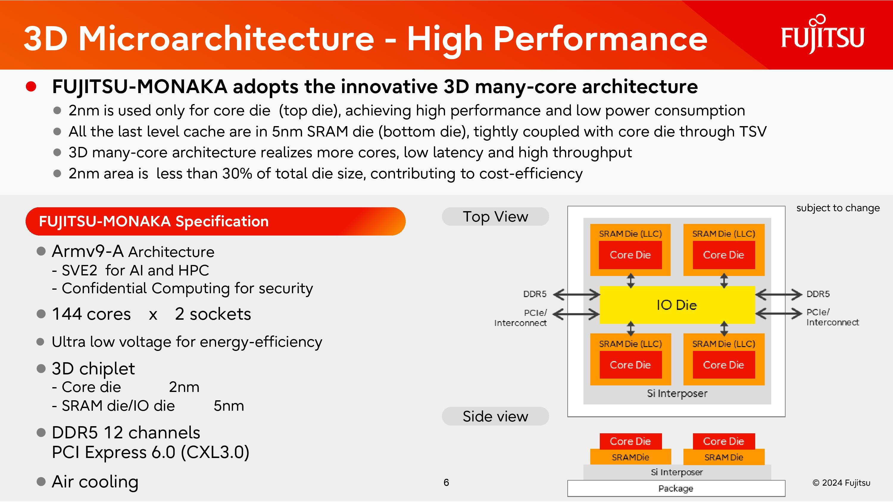
This approach reflects both ambition and restraint. Fujitsu is using cutting-edge silicon where it matters, while choosing more cost-effective and higher-yielding processes for the larger SRAM and IO dies. It’s a practical design, and one that aligns with Japan’s stated goal of energy-conscious infrastructure. Instead of pushing memory bandwidth through exotic packaging or HBM, Monaka will rely on DDR5 (twelve channels per socket) and PCIe Gen6 for high-throughput IO with CXL 3.0 support, balancing modern capability with proven standards.
From a physical standpoint, the design is dense but not exotic. The chip will likely come in under 500W with a thermal envelope suitable for standard server racks. That’s a notable departure from A64FX, which ran in liquid-cooled supercomputing environments. Here, the goal isn’t peak floating-point performance — Fujitsu says it’s about being scalable and providing efficient throughput in real-world datacenter deployments. Fujitsu isn’t trying to outgun on raw vector compute. It’s building a general-purpose server-class Arm chip with an emphasis on total platform balance.
The presentation materials at MWC included a labeled exploded view of the chip, showing core, IO, and memory dies layered and bonded with TSVs, along with a wafer mockup for visual reference. For anyone familiar with packaging trends in hyperscale silicon — from AMD’s 3D V-Cache to Intel’s Foveros — the direction is familiar. Fujitsu claims that Monaka’s emphasis on predictable power, composability, and workload isolation is what sets it apart.
Performance and Efficiency Goals
Fujitsu claims that Monaka will deliver a 2× improvement in both application performance and performance per watt generation-on-generation, projected around its planned launch window in 2027. These aren’t abstract targets. Several slides at MWC explicitly laid out the chip’s design principles: keep voltages low, optimize switching power, and scale efficiently across cores without exotic cooling or memory solutions.
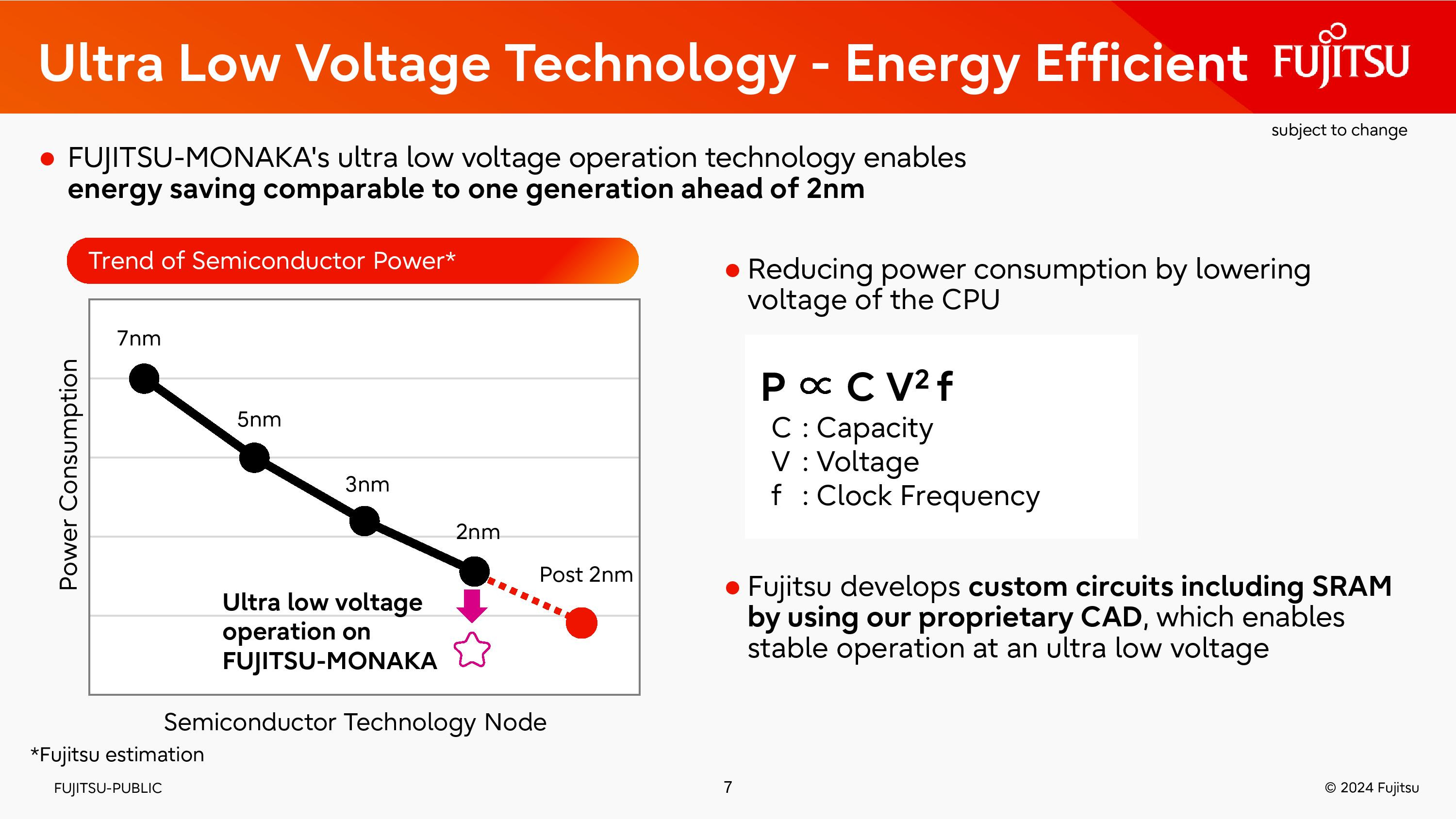
One of the central themes of Monaka’s design is ultra-low voltage operation. Fujitsu’s development materials highlighted its use of internal EDA tools to ensure stable performance at reduced voltages — a strategy the company claims offers efficiency gains comparable to advancing a full process node. Combined with the move to a 2nm gate-all-around process for the core die, this positions Monaka as a high-density, low-power compute platform.
Fujitsu’s messaging also emphasized predictability. Rather than chasing theoretical peak TOPS or FLOPS, Monaka is framed as a platform optimized for consistent, scalable performance across mixed workloads. Fujitsu is also positioning Monaka against emerging high-core-count datacenter CPUs from AMD, Intel, and others moving into Arm territory. AMD’s high core count EPYC Bergamo targets cloud-native workloads with aggressive density and performance-per-watt, while Intel’s upcoming Clearwater Forest leans heavily into E-core scalability. On the Arm side, NVIDIA’s Grace CPU Superchip and Ampere’s AmpereOne both reflect the same trend: high core count, high memory bandwidth, and lower power draw.
What sets Monaka apart, according to Fujitsu, is its emphasis on low-voltage efficiency, predictable power scaling, and a conventional server deployment model without exotic DRAM or liquid cooling. Rather than racing to peak vector compute or AI acceleration, Fujitsu is optimizing for consistent throughput and composability — a contrast to the more AI-oriented direction taken by many of its peers.
Security, Reliability, and Deployment
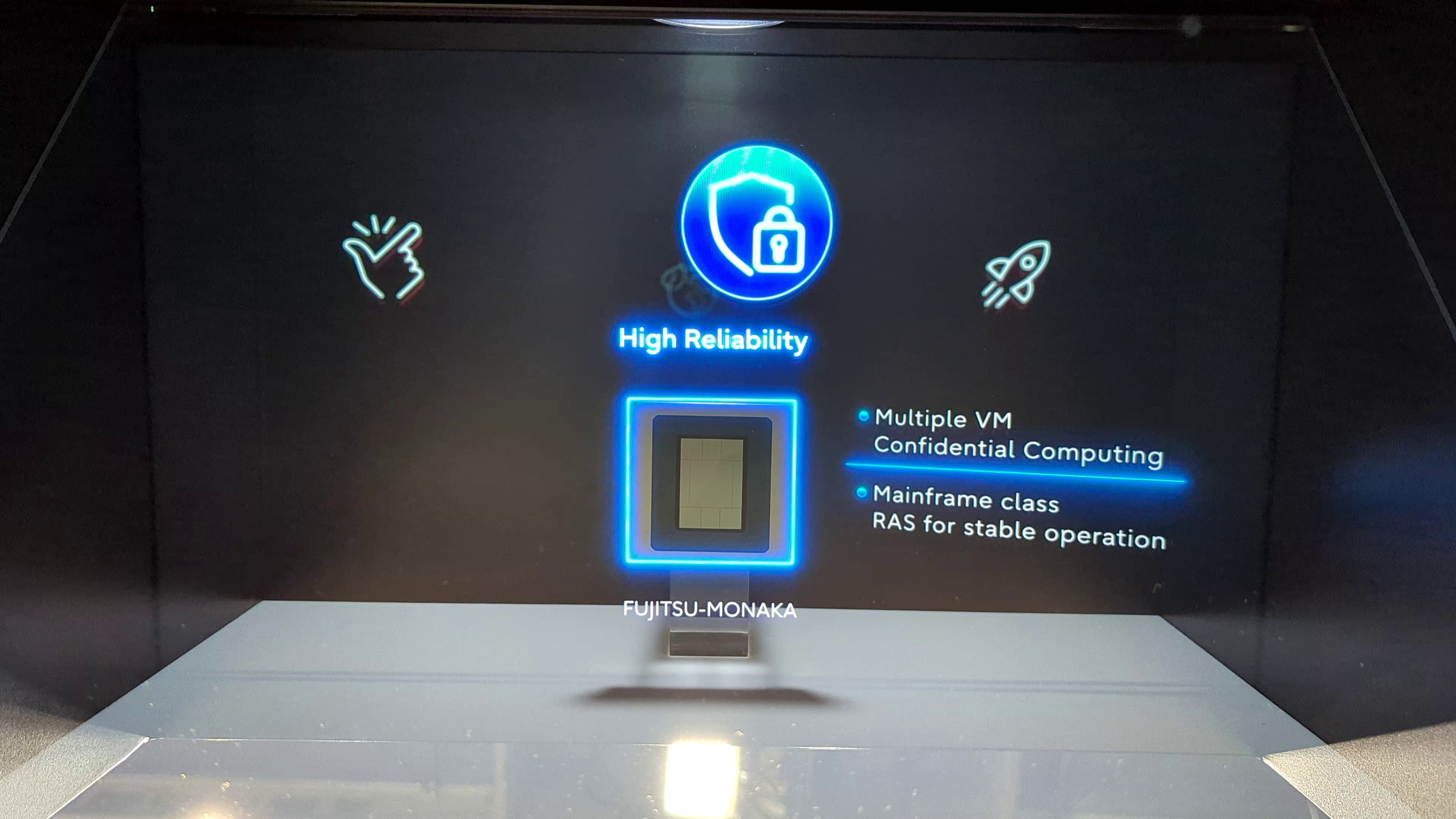
Monaka is also being designed for trust. Fujitsu’s presentation materials emphasize hardware-level isolation, workload protection, and system resilience — positioning Monaka as a platform for confidential computing in multi-tenant environments.
At the core of this is full memory encryption, with each virtual machine secured using a unique key generated and managed by hardware. Fujitsu states that these protections are implemented at boot and enforced at runtime, ensuring isolation not just between users, but between the user and the host environment itself. This aligns with the industry-wide push for confidential computing seen in platforms like AMD SEV-SNP and Intel TDX, but with Fujitsu integrating the functionality into a broader RAS-first philosophy rather than treating it as an optional module.
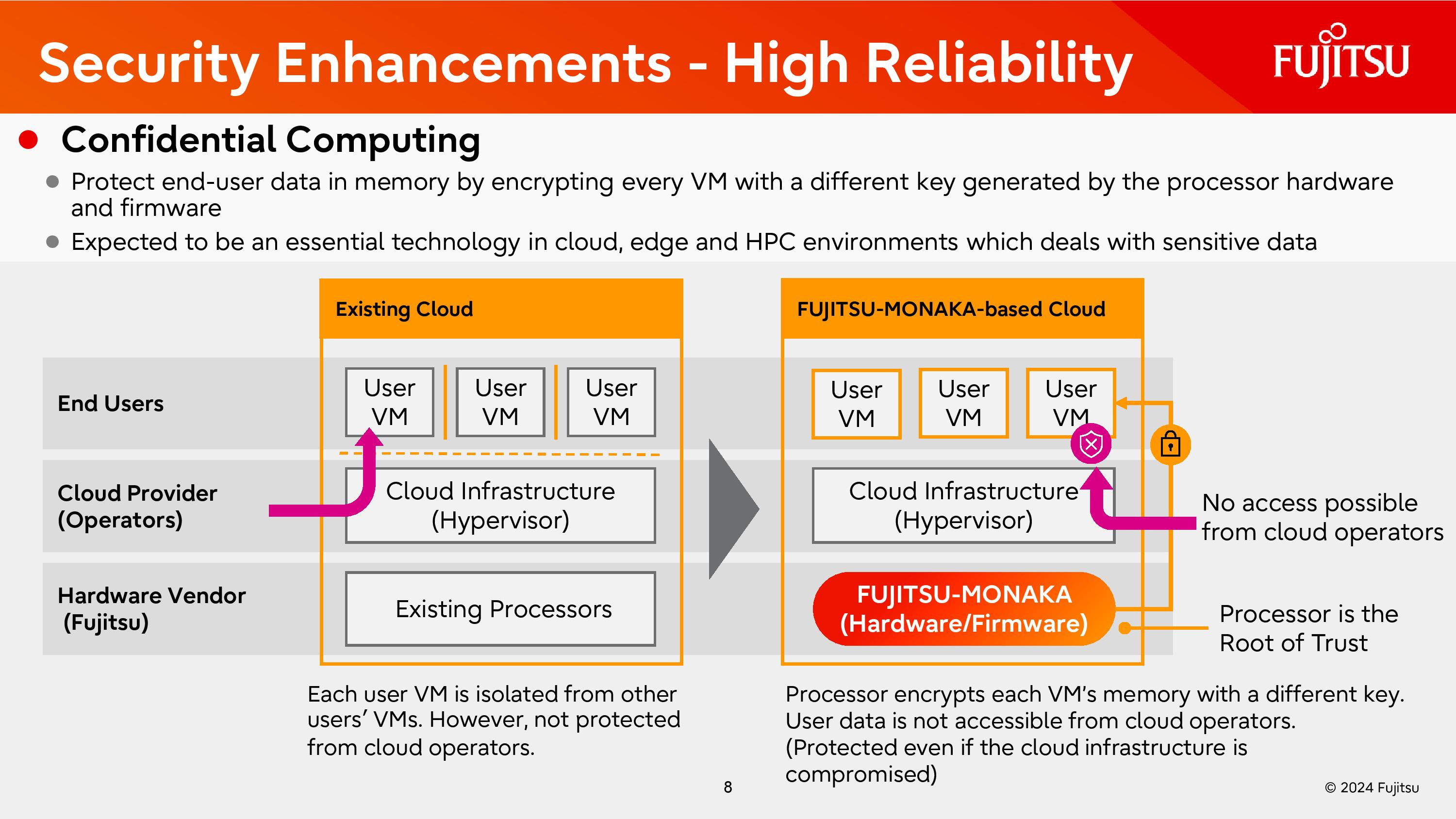
In addition to memory protection, Fujitsu describes Monaka as including a built-in hardware root of trust – a cryptographic identity embedded directly into the processor, intended to anchor system-level security and attest firmware authenticity. These features are paired with support for trusted boot and runtime integrity verification, all of which align Monaka with the requirements of high-assurance workloads in sectors like government, finance, and telco.
Reliability features are also inherited from Fujitsu’s background in mainframe and mission-critical compute. The company has referenced Monaka’s inclusion of error detection and correction mechanisms, thermal control, fault containment, and serviceability at the platform level. While specific RAS mechanisms have not been detailed publicly, Fujitsu appears to be positioning Monaka as a chip that can operate with high uptime and isolation in large-scale distributed deployments — in contrast to accelerators or dataflow engines that emphasize throughput only.
Software and Ecosystem
Fujitsu has made it clear that Monaka isn’t just a hardware project. The software environment is a core part of its design, with a focus on standards compliance, developer accessibility, and broad compatibility. Unlike some custom CPUs that require bespoke toolchains, Monaka is positioned to run a standard Linux stack, with support for upstream distributions, common development tools, and industry-wide interoperability frameworks. On top of that, Fujitsu will sprinkle its own magic with its history of compiler optimization tools.
According to Fujitsu’s public roadmap, Monaka will support Arm SystemReady SR, ensuring that the platform behaves like a conventional Arm server from a firmware and OS perspective. This makes it viable for use in sovereign cloud environments, edge deployments, and enterprise datacenters without requiring OS-level porting or vendor-specific hooks.
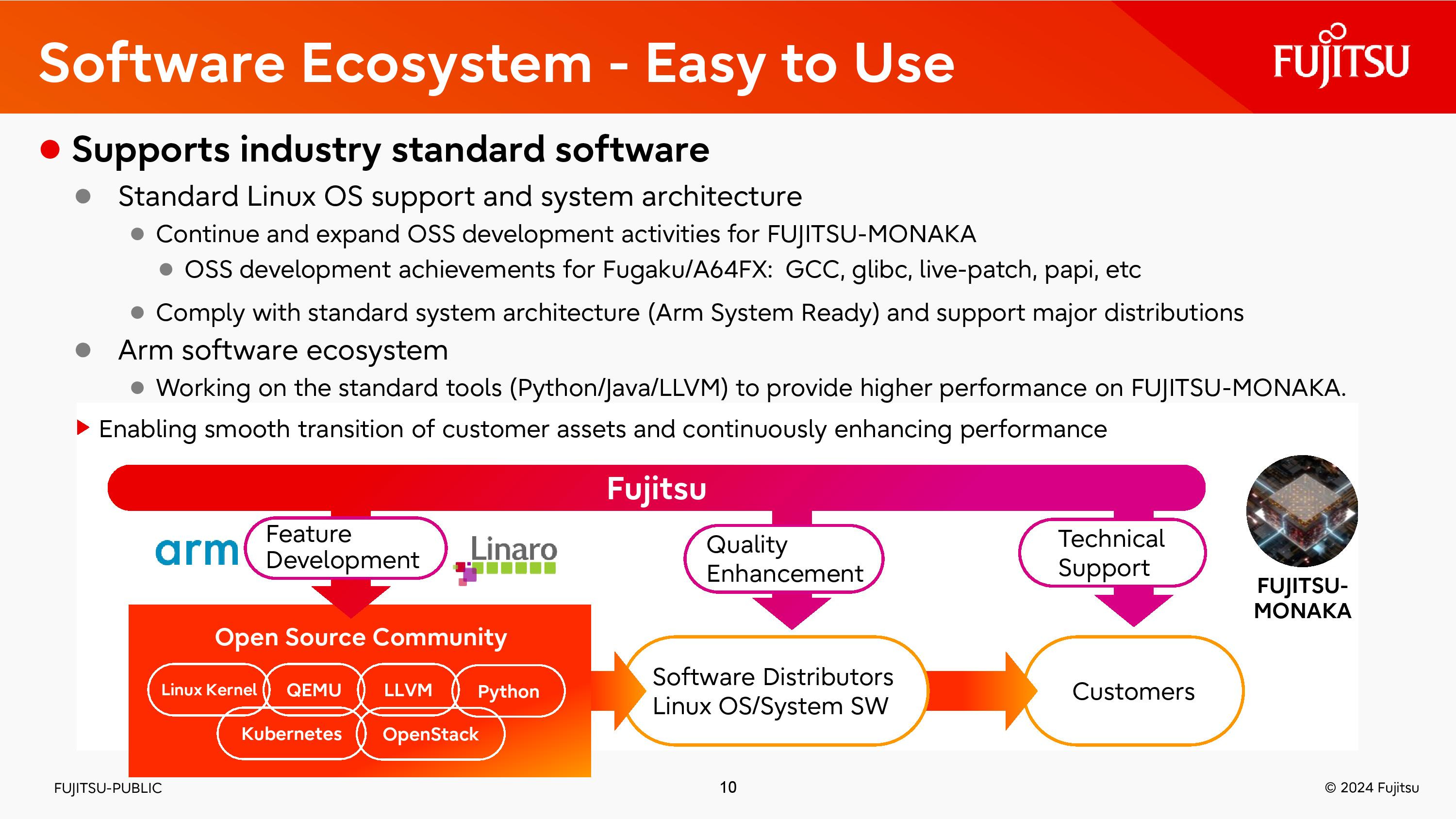
The development stack includes support for LLVM, GCC, Python, and standard performance tracing tools, consistent with the toolchain used for A64FX and the Fugaku supercomputer. Fujitsu also referenced ongoing contributions to open-source projects such as glibc, binutils, and kernel components related to power and cache management — reflecting a long-standing commitment to upstream collaboration. This positions Monaka as a server platform that existing software ecosystems can build on, rather than adapt to.
Fujitsu reiterated its support for AMD’s ROCm GPU stack – first announced in late 2024 – indicating Monaka’s role in heterogeneous infrastructure alongside AMD accelerators. While specifics weren’t disclosed, its continued presence alongside LLVM and Python reflects a broader intent: enable GPU-CPU pairing without proprietary lock-in.
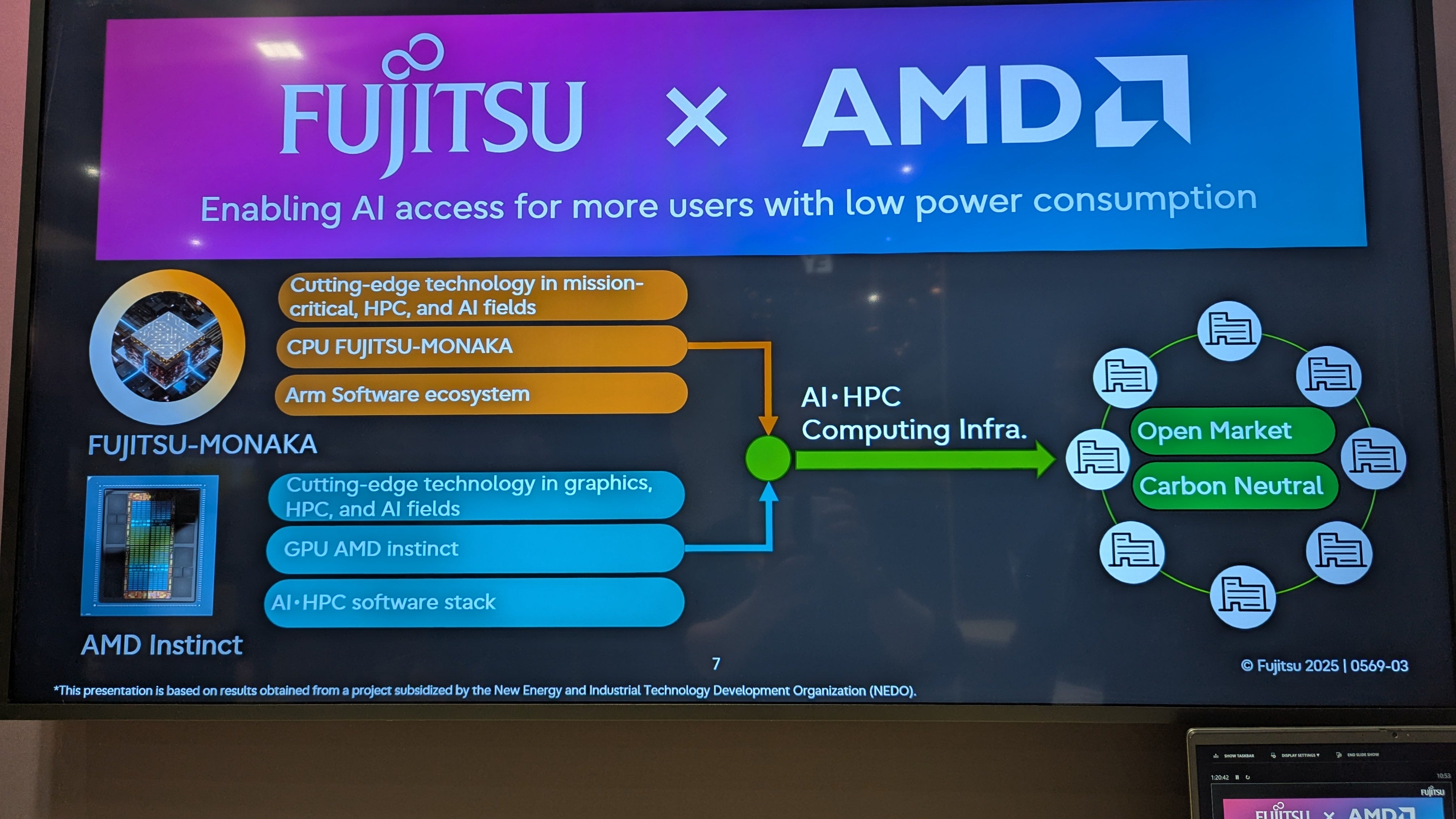
At the runtime level, Fujitsu has stated that Monaka will support CXL 3.0, enabling composable infrastructure and memory expansion beyond local DRAM. This is paired with support for PCIe Gen6, offering compatibility with next-generation storage, accelerators, and networking devices. These capabilities reflect the chip’s intended use in highly-scalable infrastructure, from cloud-native platforms to edge-hosted AI inference.
The overall message is one of continuity. Monaka isn’t being launched into a cold environment — it’s arriving into an ecosystem that Fujitsu already supports, and that much of the Arm server world already uses.
Industry Comparison
Fujitsu’s decision to describe Monaka as a “mainframe-class” processor is not common language in the Arm server world. At Mobile World Congress, the term was used alongside references to VM-level encryption, hardware root of trust, and full-system fault management — a framing that recalls enterprise platforms like IBM’s zSeries, not the usual stateless cloud compute.
IBM’s mainframes are architected for environments where uptime is contractual – banking, national ID infrastructure, transactional telco systems. Fujitsu isn’t claiming Monaka meets those specifications, but it is clearly aligning itself with that mindset. The emphasis is on predictable behaviour, lifecycle control, and secure tenancy – not simply aggregate throughput. This means Monaka’s reliability posture is broader: it’s being built to support multi-tenant systems, confidential computing, and regulated environments — the kinds of deployments that historically favored platforms like IBM’s zSeries.
Monaka doesn’t appear aimed at displacing IBM directly. The design doesn’t include proprietary interconnects or closed firmware layers, and it doesn’t assume vertically integrated middleware. What Fujitsu is proposing instead is an open, standards-based platform that offers a similar reliability envelope but with Arm compatibility, Linux-first tooling, and easier composability — especially when paired with SystemReady certification.
This makes Monaka pointed at certain markets that often sit between hyperscaler and enterprise:
-
Sovereign cloud deployments in countries seeking to control platform integrity
-
Telco networks managing regional infrastructure under strict SLAs
-
Defence and aerospace, where hardware lifecycle transparency matters more than absolute performance
Fujitsu appears to be carving out a middle ground: not chasing the hyperscale data plane, not matching IBM’s vertical stack, but building a standards-compliant platform with reliability as the product, not the pitch.
Fujitsu’s Architecture Track Record
Fujitsu’s move into mainstream datacenter silicon with Monaka doesn’t come from nowhere. The company has decades of experience designing its own processors – not as vanity projects, but as the central pillars of national-scale computing. Its SPARC64 line powered enterprise servers and mission-critical systems across Japan and beyond, with variants like the SPARC64 X and XII running everything from banking infrastructure to government compute. Fujitsu wasn’t just a user of the SPARC ISA – it was a principal architect and sustained its own implementations long after most others had moved on.
The shift to Arm began in earnest with A64FX, developed for the Fugaku supercomputer. That chip introduced 48 Armv8-A cores per socket, vector extensions via SVE, and a tightly integrated memory architecture. More importantly, it proved that Arm could scale – not just in core count, but in system-wide performance, tooling, and real-world reliability. Fugaku held the #1 spot on the TOP500 and Green500 for multiple cycles and still ranks among the most powerful and efficient machines in the world.
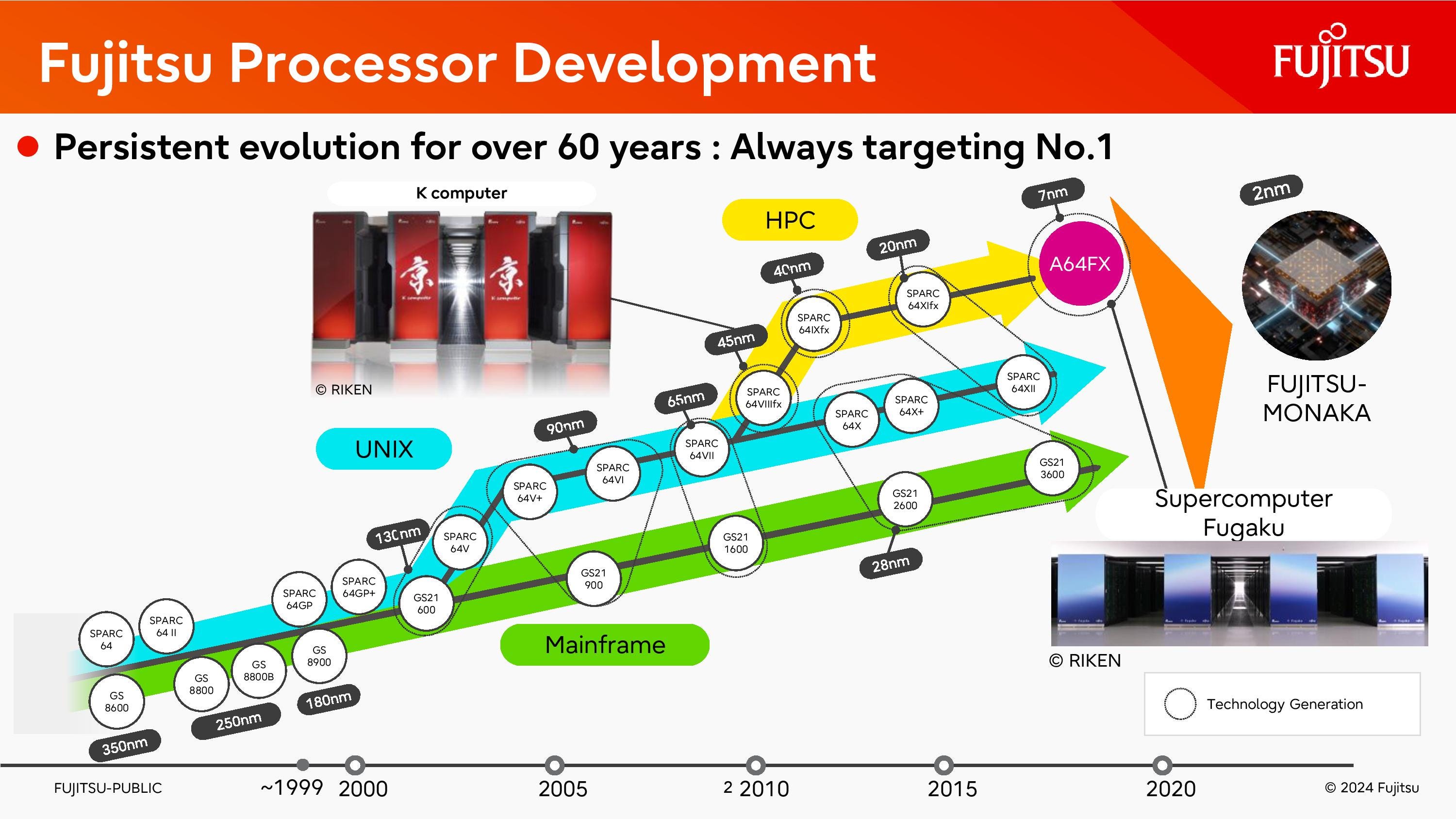
With Monaka, Fujitsu is pivoting again — not toward bleeding-edge performance per watt, but toward deployability. The core count has increased dramatically, but the vector plus HBM focus of A64FX has been replaced by composability, isolation, and a modern datacenter feature set. This evolution reflects a broader philosophy: Fujitsu builds chips not to compete on flops or flash, but to serve particular workloads with long lifetimes and well-scoped requirements. The company’s roadmap shows a clear arc from SPARC’s enterprise DNA, through A64FX’s Arm-based HPC milestone, to Monaka’s general-purpose, open-standard architecture.
Monaka may look new in the cloud CPU space, but Fujistu isn’t. Monaka is more accurately the next chapter in a 30-year design lineage that has always prioritized control, integration, and national compute capability over speed alone.
The 2nm Bet
Monaka is scheduled to arrive in fiscal 2027. That’s a long runway, so it will be interesting to see if Fujitsu not only holds to that timeframe but how the chip will be positioned against the competition at that time. On top of that, given the target markets, Fujitsu will have to provide hardware and software support on a regular cadence to a wider set of market verticals.
As for the booth section at Mobile World Congress, Fujitsu didn’t bring developer kits or run public demos. Instead, it brought slides. A silicon mockup. And an architecture that’s not trying to compete on peak performance, but on consistency, power control, and deployment trust. It was a quiet update, but a deliberate one — with every indicator pointing toward a chip designed not for one customer, but for a policy shift.
The platform takes lessons from SPARC and A64FX but breaks from both. It’s Armv9, packaged for air-cooled racks, and openly positioned for use in sovereign cloud, telco networks, and workloads where system validation and reliability still carry more weight than who has the most cores. Fujitsu says Monaka will deliver 2× the application performance and 2× the performance-per-watt compared to an unnamed 2027-era competitor. Whether that holds is secondary to what the chip actually represents: a push toward composable, secure, and standards-based infrastructure — with all the hardware control that implies.
It’s not a chip built for the spotlight — but it fits a long pattern of Fujitsu putting advanced silicon into places where reliability matters more than visibility.